
The design parameters for the BJT differential amplifier with the active load and the mode voltage gain.
Answer to Problem D11.71P
The value of the differential voltage gain is
Explanation of Solution
Given:
The given circuit is shown in Figure 1
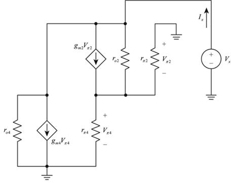
Figure 1
Calculation:
The expression for the input current is given by,
The expression to determine the value of the transconductance is given by,
The expression for the relation for the voltage for hybrid pie parameter.
Substitute
The value of the collector current
The value of the collector current
The expression to determine the expression for the diffusion resistance is given by,
Substitute
The value of the transconductance is calculated as,
Substitute
The expression to determine the value of the resistance
Substitute
The expression to determine the expression for the diffusion resistance is given by,
Substitute
The value of the transconductance is calculated as,
Substitute
The expression to determine the value of the resistance
Substitute
Substitute
The expression for the input current
Substitute
Substitute
The expression to determine the output resistance is given by,
Substitute
The value of the quiescent current is given by,
The small signal output resistance is calculated as,
The value of the output resistance is calculated as,
The required small signal circuit is shown in Figure 2
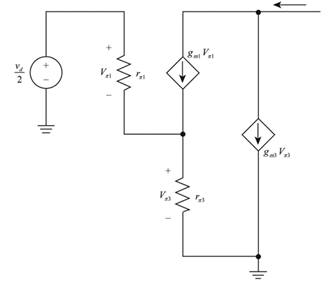
Figure 2
The expression for the transconductance is given by,
The expression for the differential voltage gain is given by,
The expression for the change in current is given by,
Consider the value of
Substitute the values in the above equation.
Substitute
Substitute
Substitute
Substitute
The value of gain is given by,
The expression for the input resistor is given by,
The value of expression for the differential input resistor is calculated as,
Conclusion:
Therefore, the value of the differential voltage gain is
Want to see more full solutions like this?
Chapter 11 Solutions
Microelectronics: Circuit Analysis and Design

- What type of biasing circuit using in the common source JFET amplifier?arrow_forwardUse a load-line analysis for the PMOS amplifier shown in Figure P11.24 to determine the maximum, minimum, and Q-point values of vo(t). The characteristics of the transistor are shown in Figure 11.9 on page 565.arrow_forwardWhat is the maximum current gain in a common-base amplifier?arrow_forward
- NOTE: FOR ALL CIRCUITS SHOWN IN THIS QUIZ ASSUME THAT: β= 100 (for all transistors) ; Early voltage equal to infinity. 3. - For the circuit shown in figure C, determine the value of the gainAv = vo/vs Note: It is known that Vcc = 20varrow_forwarda.) Consider a two-BJT configuration in Figure 1. You may assume that both transistors are the same with the same β, VBE,on = 0.7 V, and VCE,EOS = 0.3 V. Determine the minimum voltage VBE that will turn ON both Q1 and Q2. b.) Using the BJT small-signal model given in Figure 2, determine the AC current gain Ai = iout/iin for the circuit given in Figure 3. Assume ro >> rπ. You may assume that β is large.arrow_forwardHow a BJT works as an Amplifier? Explain in detail?arrow_forward
- Describe the purpose and operating principle of UJT (unijunction transitor) and SCR amplifiersarrow_forwardNOTE: FOR ALL CIRCUITS SHOWN IN THIS QUIZ ASSUME THAT: β= 100 (for all transistors) ; Early voltage equal to infinity. 2. - For the circuit shown in figure B, determine:a) The values of IcQ and VceQ for Q1 and Q2b) The input resistance Ri and the output resistance Roarrow_forward2- Draw a transistor amplifier circuit ( BJT ) Bipolar Junction of type ( NPN ) then write the mathematical relation of Circuit voltage gain factor and what is the factors that depend on and how can we increase the gain factor .arrow_forward
- What are the advantages of using a Differential rather than a Single-Transistor Amplifier? Explain the operation of Operation amplifier as summer and integrator?arrow_forwardThe transistor parameters for the NMOS common source amplifier given in the figure are VTN = 1.0V, kn = 0.8mA / V2 and alpha = 0. Circuit parameters are VDD = 10V, RS = 0.8k, RD = 3K, R1 = 210K and R2 = 140k. Find the IDQ drain current and VDSQ drain-source voltage at the transistor's Q - operating point. Determine in which region the transistor is operating.arrow_forwardQ.1/ Figure below shows a CE power amplifier in which the collector resistor serves also as the load resistor. Assume DC=ac=100.a. Determines the dc Q-point (ICQ and VCEQ).b. Determine the voltage gain and the power gain.c. What changes would be necessary to convert the circuit to a pnp transistor with a positive supply? What advantage would this have?arrow_forward
 Introductory Circuit Analysis (13th Edition)Electrical EngineeringISBN:9780133923605Author:Robert L. BoylestadPublisher:PEARSON
 Delmar's Standard Textbook Of ElectricityElectrical EngineeringISBN:9781337900348Author:Stephen L. HermanPublisher:Cengage Learning
 Programmable Logic ControllersElectrical EngineeringISBN:9780073373843Author:Frank D. PetruzellaPublisher:McGraw-Hill Education
 Fundamentals of Electric CircuitsElectrical EngineeringISBN:9780078028229Author:Charles K Alexander, Matthew SadikuPublisher:McGraw-Hill Education
 Electric Circuits. (11th Edition)Electrical EngineeringISBN:9780134746968Author:James W. Nilsson, Susan RiedelPublisher:PEARSON
 Engineering ElectromagneticsElectrical EngineeringISBN:9780078028151Author:Hayt, William H. (william Hart), Jr, BUCK, John A.Publisher:Mcgraw-hill Education,