
Videos
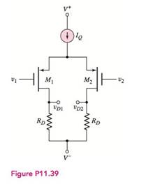
Consider the circuit shown in Figure P 11.39 . The circuit and transistor parameters are
Want to see the full answer?
Check out a sample textbook solution
Chapter 11 Solutions
Microelectronics: Circuit Analysis and Design


- V* = + |ov Ri Rip ERC Vs RE V: -sV The following parameters are given for this transistor: B = 200 and VA = o. Design the circuit with the following value ICQ = 1.5mA and VCEQ = 5V. Find the small signal voltage gain AV = Vo/Vs. Find the input resistance in the signal source Vs.arrow_forwardFind the parameters from this circuit Parameters ..beta , re , IEQarrow_forward1. For the circuit in Figure 1: a) Calculate the input and output power if the input signal results in a base current of 5 mA rms. b) Calculate the input power dissipated by the circuit if Rg is changed to 1.5 kN. c) What maximum output power can be delivered by the circuit if RB is changed to 1.5 kN? d) If the circuit is biased at its center voltage and center collector operating point, what is the input power for a maximum output power of 1.5 W? +Vcc (18 V) Rc = 16 2 RB 1.2 k2 V. B - 40 100 µF Figure 1arrow_forward
- QUESTION 16: For the transistors in the circuit in Figure 11.32, the circuit parameters V* = 1.8V, V = −1.8V, and IQ = 155 μA. The transistor parameters are: k'n = 100 µA/V², k'p = 40 µA/V², VĨN = 0.3V, Vpp = −0.3V, (W/L)n = 8, (W/L)p = 10, λp = 35 mV¯¹, and λñ = 27 mV¯¹. Determine the small signal differential-mode voltage gain, Ad ro2₂ (k)| Format: 666.3325280404 704 (kn) Format: 583.38844987004 Ad Format: 73.235927554867 M₁ V10- ip3 M3 fiDi M₁ V+ V™ lo iD2 M₂ iD4 -OVO V₂arrow_forwardIn the circuit shown in Figure 1, the input signal vsig is a small sine-wave signal with zeroaverage. The transistor β is 100.Figure 1: BJT Amplifier(a) For RL = 10KΩ, draw the small-signal equivalent circuit of the amplifier and determineits overall voltage gain.(b) What is the input resistance of the amplifier circuit?arrow_forward6) the "simplest" model of transistor behavior in this problem, i.e., B = o and IB = 0, with forward bias voltage of AVBE = 0.6V. Consider the following circuit with a transistor and two resistors. You may use 5V a) Determine the output when Vin = 0.5V. 9kN Vout Vin 3002 3kN b) Determine the output when Vin = 1.2 V. c) Determine the output when Vin = 3.6 V.arrow_forward
- ........ (Figure-1) R. RB= 380kN,Rc= 1kN B = 100, VBB = Vcc=12V RB ww Vec CC ......... I, V CE СЕ V ВЕ BB Q-1-b) Describe briefly the input / output characteristics and application of Common Emitter BJT Configurationarrow_forwardK = 2 mA/V, V, = -3 V ve Vpp = 50 V Rp=8 k2 a) Calculate the ID current and VDS voltage. 100 2 b) Draw the small signal equivalent circuit of the circuit. 4kS 50 ka 250 2 c) Calculate the input impedance of Rin. d) Calculate the gain of the circuit.arrow_forward5, a) Determine Vdsat when ID=.5 mA. b) Determine Kn when ID = 0.5 Amps. (Show your work!) c) Determine VTN. (Show your work!) d) Vgs Consider the circuit and corresponding graph, shown below. ID (mA) 0.60 0.50 0.40 0.30 0.20 0.10 0.00 0 0.5 Vds 1 1.5 2 2.5 Vds 3 3.5 4 4.5 5 -Vgs = 1V - Vgs = 1.1V - Vgs = 1.2V - Vgs = 1.3Varrow_forward
- Q.1 (a) Figure Q.1(a) is a voltage regulator with a foldback protection circuit at its output with input voltage, VIN varies from 15 V to 20 V. The transistor parameters are : Q₁: VBEI(on) 1.2 V and B₁ = 50 25 Q2: VBEZ(on) 0.7 V and B₁=200 (i) ww (ii) Using the foldback circuit, derive the expression of the maximum current, IL(max) and the short circuit current, Iusc. Calculate their values when Vo is set to 15 V. Determine the minimum and maximum values for the output voltage Vo. (iii) Calculate the maximum power dissipated in pass transistor Q when the output is short-circuited. 25 15 V ≤ VN 525 V R$ 4700 V₂ 6.8 V www R₁ VB1 www R₂c ww 192 R4 2000 ww R$ 8000 Figure Q.1(a): Foldback Voltage Regulator Circuit www R₁ 5.6 ΚΩ R₂ 10 k R₂ 6.8 k R₂arrow_forwardThe transistor parameters for the circuit in Figure P11.9 are: B = 100, VBE (On) = 0.7 V, and VA = ∞o. (a) Determine RE such that IE = 150 μΑ. (b) Find Ad, Acm, and CMRRB for a one-sided output at vo2. (c) Determine the differential- and common-mode input resistances. Rc-50 k Rg = 0.5 kΩ www VI www 21 Figure P11.9 +10 V VOLVO2 IE RE -10 V ? Rc = 50 kΩ 22 Rg = 0.5 kΩ ww S'arrow_forwardThe circuit shown above is the ac model for a Common Collector amplifier. Determine the value of the following circuit elements. a) ro b) RE c) RL d) gm e) RB f) rπ g) Rsigarrow_forward
 Introductory Circuit Analysis (13th Edition)Electrical EngineeringISBN:9780133923605Author:Robert L. BoylestadPublisher:PEARSON
 Delmar's Standard Textbook Of ElectricityElectrical EngineeringISBN:9781337900348Author:Stephen L. HermanPublisher:Cengage Learning
 Programmable Logic ControllersElectrical EngineeringISBN:9780073373843Author:Frank D. PetruzellaPublisher:McGraw-Hill Education
 Fundamentals of Electric CircuitsElectrical EngineeringISBN:9780078028229Author:Charles K Alexander, Matthew SadikuPublisher:McGraw-Hill Education
 Electric Circuits. (11th Edition)Electrical EngineeringISBN:9780134746968Author:James W. Nilsson, Susan RiedelPublisher:PEARSON
 Engineering ElectromagneticsElectrical EngineeringISBN:9780078028151Author:Hayt, William H. (william Hart), Jr, BUCK, John A.Publisher:Mcgraw-hill Education,