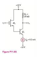
Problem 11.1EP: The circuit parameters for the differential amplifier shown in Figure 11.2 are V+=5V,V=5V,IQ=0.3mA,... Problem 11.2EP: Consider the de transfer characteristics shown in Figure 11.5 . Determine the value of the... Problem 11.1CSP Problem 11.3EP: Consider the diff-amp described in Example 11.3 . Assume the same circuit and transistor parameters... Problem 11.4EP Problem 11.1TYU Problem 11.2TYU Problem 11.3TYU: Assume the differential-mode gain of a diff-amp is Ad=80 and the common-mode gain is Acm=0.20.... Problem 11.5EP Problem 11.6EP: Consider the diff-amp shown in Figure 11.15 . Assume the current source has a value of IQ=0.5mA, the... Problem 11.7EP Problem 11.4TYU Problem 11.5TYU Problem 11.6TYU: The parameters of the diff-amp shown in Figure 11.2 are V+=5V V=5V,IQ=0.4mA, and RC=10k. The output... Problem 11.8EP: For the differential amplifier in Figure 11.20, the parameters are: V+=5V,V=5V,R1=80k, and RD=40k.... Problem 11.9EP: The parameters of the circuit shown in Figure 11.19 are V+=3V V=3V,IQ=0.2mA, and RD=15k. Assume M1... Problem 11.7TYU: The circuit parameters of the diff-amp shown in Figure 11.19 are V+=3V,V=3V,IQ=0.40mA, and RD=7.5k.... Problem 11.8TYU: Consider the differential amplifier in Figure 11.20 . The transistor parameters are given in Example... Problem 11.9TYU: The diff-amp in Figure 11.19 is biased at IQ=100A. The transistor parameters are kn=100A/V2 and... Problem 11.10TYU Problem 11.10EP: The diff-amp circuit in Figure 11.30 is biased at IQ=0.4mA. The transistor parameters are... Problem 11.11EP Problem 11.12EP Problem 11.11TYU Problem 11.12TYU Problem 11.13TYU: Redesign the circuit in Figure 11.30 using a Widlar current source and bias voltages of 5V . The... Problem 11.14TYU Problem 11.15TYU Problem 11.16TYU Problem 11.17TYU Problem 11.13EP: Consider the Darlington pair Q6 and Q7 in Figure 11.46 . Determine the current gain of the... Problem 11.14EP Problem 11.18TYU: Consider the Darlington pair and emitter-follower portions of the circuit in Figure 11.46 . The... Problem 11.19TYU Problem 11.15EP Problem 11.16EP: Consider the simple bipolar op-amp circuit in Figure 11.49 with circuit and transistor parameters... Problem 11.17EP Problem 1RQ: Define differential-mode and common-mode input voltages. Problem 2RQ Problem 3RQ: From the dc transfer characteristics, qualitatively define the linear region of operation for a... Problem 4RQ: What is meant by matched transistors and why are matched transistors important in the design of... Problem 5RQ Problem 6RQ: Explain how a common-mode output signal is generated. Problem 7RQ: Define the common-mode rejection ratio, CMRR. What is the ideal value? Problem 8RQ: What design criteria will yield a large value of CMRR in an emitter-coupled pair? Problem 9RQ Problem 10RQ: Define differential-mode and common-mode input resistances. Problem 11RQ: Sketch the de transfer characteristics of a MOSFET differential amplifier. Problem 12RQ: Sketch and describe the advantages of a MOSFET cascode current source used with a MOSFET... Problem 13RQ Problem 14RQ Problem 15RQ: Describe the loading effects of connecting a second stage to the output of a BIT diff-amp. Problem 16RQ Problem 17RQ Problem 18RQ Problem 11.1P: (a) A differential-amplifier has a differential-mode gain of Ad=250 and a common-mode rejection... Problem 11.2P Problem 11.3P: Consider the differential amplifier shown in Figure P 11.3 with transistor parameters... Problem 11.4P Problem D11.5P Problem 11.6P: The diff-amp in Figure 11.3 of the text has parameters V+=+5V V=5V,RC=8k, and IQ=0.5mA. The... Problem D11.7P: The diff-amp configuration shown in Figure P11.7 is biased at 3V . The maximum power dissipation in... Problem 11.8P: Consider the circuit in Figure P11.8, with transistor parameters: =100 VBE(on)=0.7V, and VA=. (a)... Problem 11.9P: The transistor parameters for the circuit in Figure P11.9 are: =100 VBE(on)=0.7V, and VA=.(a)... Problem 11.10P Problem 11.11P Problem 11.12P: The circuit and transistor parameters for the circuit shown in Figure P 11.11 are... Problem 11.13P Problem 11.14P: Consider the differential amplifier shown in Figure P11.14 with mismatched transistors. The... Problem 11.15P: Consider the circuit in Figure P11.15. The transistor parameters are =120,VEB(on)=0.7V, and VA=.... Problem 11.16P Problem 11.17P Problem 11.18P: For the diff-amp in Figure 11.2, determine the value of vd=v1v2 that produces (a) iC1=0.20IQ and (b)... Problem 11.19P Problem D11.20P Problem 11.21P Problem 11.22P: The circuit parameters of the diff-amp shown in Figure 11.2 are V+=3V,V=3V, and IQ=0.25mA. Base... Problem 11.23P: Consider the circuit in Figure P11.23. Assume the Early voltage of Q1 and Q2 is VA=, and assume the... Problem 11.24P Problem 11.25P: Consider the small-signal equivalent circuit of the differential-pair configuration shown in Figure... Problem D11.26P Problem 11.27P Problem 11.28P: A diff-amp is biased with a constant-current source IQ=0.25mA that has an output resistance of... Problem 11.29P: The transistor parameters for the circuit shown in Figure P 11.29 are =180,VBE(on)=0.7V (except for... Problem D11.30P Problem 11.31P: For the differential amplifier in Figure P 11.31 the parameters are R1=50k and RD=24k. The... Problem 11.32P Problem 11.33P Problem 11.34P Problem 11.35P Problem 11.36P Problem 11.37P: Consider the normalized de transfer characteristics of a MOSFET diff-amp shown in Figure 11.21 .... Problem 11.38P Problem 11.39P: Consider the circuit shown in Figure P 11.39 . The circuit and transistor parameters are V+=+3 V,... Problem 11.40P Problem 11.41P Problem 11.42P Problem 11.43P Problem D11.44P Problem D11.45P Problem 11.46P Problem 11.47P: Consider the circuit shown in Figure P 11.47 . Assume that =0 for M1 and M2. Also assume an ideal... Problem 11.48P Problem 11.49P Problem 11.50P Problem 11.51P: Consider the MOSFET diff-amp with the configuration in Figure P11.33. The circuit parameters are... Problem 11.52P: Consider the bridge circuit and diff-amp described in Problem 11.27 . The BJT diff-amp is to be... Problem D11.53P Problem 11.54P Problem 11.55P Problem 11.56P: Consider the JFET diff-amp shown in Figure P11.56. The transistor parameters are: IDSS=0.8mA,=0, and... Problem 11.57P Problem 11.58P Problem D11.59P Problem 11.60P: The differential amplifier shown in Figure P 11.60 has a pair of pnp bipolars as input devices and a... Problem 11.61P Problem 11.62P: Consider the diff-amp shown in Figure P 11.62 . The circuit parameters are V+=3V,V=3V, and IQ=0.4mA.... Problem 11.63P Problem 11.64P: The differential amplifier in Figure P11.64 has a pair of PMOS transistors as input devices and a... Problem 11.65P Problem 11.66P: Consider the diff-amp with active load in Figure P11.66. The Early voltages are VAN=120V for Q1 and... Problem 11.67P: The diff-amp in Figure P 11.67 has a three-transistor active load circuit and a Darlington pair... Problem 11.68P: Consider the diff-amp in Figure P11.68. The PMOS parameters are: Kp= 80A/V2,p=0.02V1,VTP=2V. The... Problem 11.69P Problem 11.70P Problem D11.71P Problem D11.72P Problem D11.73P: An all-CMOS diff-amp, including the current source circuit, with the configuration in Figure 11.32... Problem D11.74P Problem 11.75P: Consider the fully cascoded diff-amp in Figure 11.37 . Assume IQ=80A and transistor parameters of:... Problem 11.76P: Consider the diff-amp that was shown in Figure P11.63. The circuit and transistor parameters are... Problem 11.77P Problem 11.78P Problem 11.79P Problem 11.80P Problem 11.81P: Consider the BiCMOS diff-amp in Figure 11.44 , biased at IQ=0.4mA . The transistor parameters for M1... Problem 11.82P: The BiCMOS circuit shown in Figure P11.82 is equivalent to a pnp bipolar transistor with an infinite... Problem 11.83P Problem 11.84P Problem 11.85P: For the circuit shown in Figure P11.85, determine the small-signal voltage gain, Av=vo/vi. Assume... Problem 11.86P: The output stage in the circuit shown in Figure P 11.86 is a Darlington pair emitter-follower... Problem 11.87P Problem 11.88P: Consider the circuit in Figure P11.88. The bias currents I1 and I2 are such that a zero de output... Problem 11.89P Problem 11.90P: Consider the multistage bipolar circuit in Figure P 11.90, in which de base currents are negligible.... Problem D11.91P Problem 11.92P Problem 11.93P: For the transistors in the circuit in Figure P11.93, the parameters are: Kn=0.2mA/V2,VTN=2V, and... Problem 11.94P Problem 11.95P Problem 11.96P Problem 11.97P: Consider the diff-amp in Figure 11.55 . The circuit and transistor parameters are the same as in... Problem D11.105DP: The transistor parameters for the circuit in Figure P11.105 are: Kn= 0.2mA/V2,VTN=0.8V, and =0. The... format_list_bulleted


 Introductory Circuit Analysis (13th Edition)Electrical EngineeringISBN:9780133923605Author:Robert L. BoylestadPublisher:PEARSON
 Delmar's Standard Textbook Of ElectricityElectrical EngineeringISBN:9781337900348Author:Stephen L. HermanPublisher:Cengage Learning
 Programmable Logic ControllersElectrical EngineeringISBN:9780073373843Author:Frank D. PetruzellaPublisher:McGraw-Hill Education
 Fundamentals of Electric CircuitsElectrical EngineeringISBN:9780078028229Author:Charles K Alexander, Matthew SadikuPublisher:McGraw-Hill Education
 Electric Circuits. (11th Edition)Electrical EngineeringISBN:9780134746968Author:James W. Nilsson, Susan RiedelPublisher:PEARSON
 Engineering ElectromagneticsElectrical EngineeringISBN:9780078028151Author:Hayt, William H. (william Hart), Jr, BUCK, John A.Publisher:Mcgraw-hill Education,