
Concept explainers
Videos
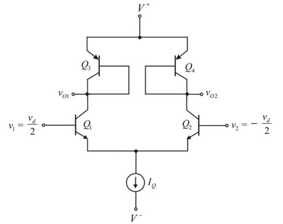
Consider the diff-amp shown in Figure P 11.62 . The circuit parameters are
(a)
To sketch: The small signal equivalent circuit for the differential amplifier.
Answer to Problem 11.62P
The small signal circuit is shown in Figure 2.
Explanation of Solution
Given:
The given circuit is shown below.

Calculation:
The small signal equivalent circuit for the above circuit is shown in Figure 1.
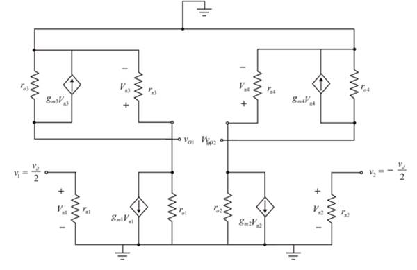
Figure 1
Because of symmetry the value of the currents
The value of the currents
The value of the currents
The value of the currents
For differential up circuit emitter current
Modify the circuit, the required diagram is shown in Figure 2
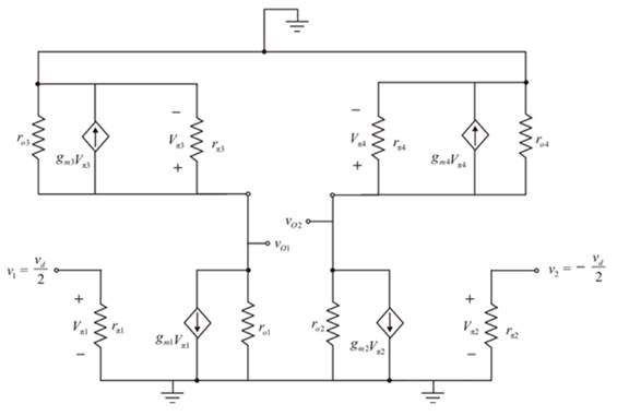
Figure 2
Conclusion:
Therefore, the small signal circuit is shown in Figure 3
(b)
The value of one sided differential voltage gain.
Answer to Problem 11.62P
The value of the differential mode voltage gain is
Explanation of Solution
Given:
The given circuit is shown below.
 Calculation:
Consider the left portion of the circuit as,
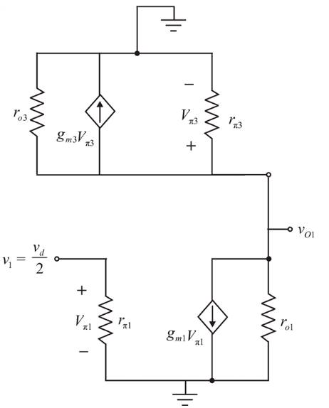
Figure 3
Modify the circuit as shown in Figure 4
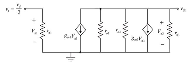
Figure 4
The expression for the output voltage of the above circuit is given by,
The emitter current of the transistor is calculated as,
The expression for the collector current of the transistor
Substitute
Apply KCL at the output node
Substitute
The transconductance of transistor
The transconductance of transistor
The small signal output resistance of
The small signal output resistance of
The small signal resistance
The value of the voltage
Conclusion:
Therefore, the value of the differential mode voltage gain is
(c)
The differential voltage gain of both the sides.
Answer to Problem 11.62P
The value of differential voltage gain is
Explanation of Solution
Given:
The given circuit is shown below.

Calculation:
The expression for the output voltage of the above circuit is given by,
The value of the voltage
Conclusion:
Therefore, the value of differential voltage gain is
(d)
The value of the differential voltage gain of both the sides.
Answer to Problem 11.62P
The value of differential voltage gain is
Explanation of Solution
Given:
The given circuit is shown below.

Calculation:
The expression to determine the value of the two sided differential voltage gain is given by,
Conclusion:
Therefore, the value of differential voltage gain is
Want to see more full solutions like this?
Chapter 11 Solutions
Microelectronics: Circuit Analysis and Design


- In the circuit given in the figure, Vcc = 15V, R1 = R2 = 10k ohm, RE = 1k ohm, RL = 0.5k ohm and transistor parameters are given as VBE = 0.7V, beta (dc) = beta (0) = 100. According to this;a) Calculate the values of DC bias currents and voltages (I (BQ), I (CQ), V (CEQ)).b) Using the hybrid model of the transistor, draw the small signal equivalent circuit of the circuit.c) Derive the input impedance expression of the circuit and calculate its value.d) Derive the voltage gain expressions A (vi) and A (VG) and calculate its value.e) Derive the current gain expression A (i) = I (0) / I (i) and calculate its value. I sent you question's image. Thank you..arrow_forward2. A load of 8Ω is supplied by a single-switch Direct Current (DC) chopper with an inputvoltage of 40V. The switching frequency is 800Hz, the duty ratio is 0.4, and thetransmission voltage drop of the transistor is 2.4V a. Draw the chopper circuit presented in the question b. Find the switching period with the duty time of BJT c. Draw the load voltage, load current, BJT current, BJT voltage along two periods d. Find the output voltage. Is the achieved load voltage the average value or the effectivevalue e. Find the output power f. Find the average value and effective value of BJT current g. Find the power loss of BJT h. Find the DC source current i. Find the circuit efficiencyarrow_forwardIn the push-pull stage given (in the photo attached), IS1 = 5 × 10⁻¹⁷ A and IS2 = 8 × 10⁻¹⁷ A. Calculate the value of VB so as to establish a bias current of 5 mA in Q1 and Q2 (for Vout = 0). If the peak input swing is 2 V and RL = 8Ω : Calculate the small-signal voltage gain for Vout ≈ 0 Use the gain obtained in (i) to estimate the output voltage swing. Estimate the peak collector current of Q1 assuming that Q2 still carries 5 mAarrow_forward
- Design the reference as shown to produce an output current IO =75μA. Assume VDD =5V and use the transistor parameters R1 = 10 kΩ, R2 = 20 kΩ, Kn =250 μA/V2, VTN =0.75 V, λ =0.017 V−1, and VDD =10 V?arrow_forwardTopic: Field Effect Transistor Given the FET Amplifier circuit. Answer the question asked in each letter. a. Transconductance Gain (gm) b. Drain Resistor (RD) c. Input Impedance (Zi) d. Output Impedance (Zo) e. Voltage Gain (Av) f. What is the AC configuration of the amplifier?common source, common gate, common drain, or source bias?arrow_forwardThe given circuit is a 2N4403 PNP common collector amplifier. Let VCC=12V, VEE=-12V, R1=52.5kΩ, R2=33kΩ, and RE=2.5kΩ. Determine IB, IC, IE, VB, VC, and VE. Start by initially assuming |VBE| =0.7V or and assuming a value of beta (β). Where to look for the value of β? (Hint: It’s in the transistor model assigned). Determine the input voltage (may extend from the supply voltage range) where the BJT goes from “cut-off to active” and where it goes from “active to saturation”. Assume VCE=0.3V (edge of saturation), RL=500Ω, and C1, C2→∞.arrow_forward
- 1. Describe the high frequency response and phase shift for BJT and FET transistors using MillersTheorem ata) Input RC circuitb) Output RC circuit The subject : Analogue Electronics IIarrow_forwardFor the BJT amplifier circuit of figure below with the following parameters:β = hfe ≈ 250, re= 20.3Ω, and ro = 1/hoe ≈ ∞ Ω, Zb= 50.26KΩ determine:(a) Draw the Ac equivalent circuit in re- model and hybrid model.(b) hie, , Zi , and Zo'(c) Av using h- model.(d) Avs and ac output voltagearrow_forwardPlease answer as soon as possible. I'll upvote it. Thanks. Consider a two-BJT configuration in Figure 1. You may assume that both transistors are the same with the same β, VBE,on = 0.7 V, and VCE,EOS = 0.3 V. Derive the DC current gain AI = IC/IB in terms of β for the two-transistor circuit. You may assume that β is large.arrow_forward
- Design the bias circuit to give aQ-point of IC = 20 μA and VC E = 0.90 V ifthe transistor current gain is βF = 50 and VB E =0.65 V. What is the Q-point if the current gain ofthe transistor is actually 125?arrow_forwardInstruction/s: Draw, Illustrate and label your schematic diagram before solving the problem.2.) Given a Collector -Feedback Biased transistor circuit with voltage at common collector is +10v ,base resistor is 100k ohms, Collector resistor is 10k ohms and Base current is 8.38 micro ampere, ,Voltage at Base-emitter junction is 0.7v. Determine Beta DC , Collector current and Voltage at collector-emitter junction. These might help as a guide to answer the problem...arrow_forward1. Derive the Avf, Rif, Rof, R’of for the circuit shown in figure 1. For each transistor theh-parameters, hie and hfe are equal.arrow_forward
 Introductory Circuit Analysis (13th Edition)Electrical EngineeringISBN:9780133923605Author:Robert L. BoylestadPublisher:PEARSON
 Delmar's Standard Textbook Of ElectricityElectrical EngineeringISBN:9781337900348Author:Stephen L. HermanPublisher:Cengage Learning
 Programmable Logic ControllersElectrical EngineeringISBN:9780073373843Author:Frank D. PetruzellaPublisher:McGraw-Hill Education
 Fundamentals of Electric CircuitsElectrical EngineeringISBN:9780078028229Author:Charles K Alexander, Matthew SadikuPublisher:McGraw-Hill Education
 Electric Circuits. (11th Edition)Electrical EngineeringISBN:9780134746968Author:James W. Nilsson, Susan RiedelPublisher:PEARSON
 Engineering ElectromagneticsElectrical EngineeringISBN:9780078028151Author:Hayt, William H. (william Hart), Jr, BUCK, John A.Publisher:Mcgraw-hill Education,