
Videos
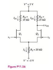
Consider the JFET diff-amp shown in Figure P11.56. The transistor parameters are:
Want to see the full answer?
Check out a sample textbook solution
Chapter 11 Solutions
Microelectronics: Circuit Analysis and Design


- Given a D-MOSFET circuit used as an amplifier with the following parameter: IDSS=12mA and a transconductance of gm=3.2 mS. Determine the DC drain to source voltage VDS and the AC output voltage if Vin=500 mV.arrow_forward"It is desirable for the following circuit, assuming the transistors are the same." A) Common fashion gain B) Differential gain mode C) Input resistance network D) CMRR E) What effect does the change in load resistance have on the circuit? Vcc Rc Re Qu, Vi PEE -VEEarrow_forward(ii) Calculate the RB, Rc, and the minimum power rating of the transistor (Note: the actual power rating should be greater).arrow_forward
- Open with v Consider class-A emitter follower circuit shown in the figure below. The circuit parameters are V+ = 24 V, V- = -24 V, and RL = 2000. The transistor parameters are B = 50, VBElon) = 0.7 V, and VCElsat) = 0.2 V. The output voltage is to vary between +20 V and -20 V. The minimum current in Q1 is to be ie1 = 20 mA. For vo = 0, find the power dissipated in the first transistor Q1- V+arrow_forward........ (Figure-1) R. RB= 380kN,Rc= 1kN B = 100, VBB = Vcc=12V RB ww Vec CC ......... I, V CE СЕ V ВЕ BB Q-1-b) Describe briefly the input / output characteristics and application of Common Emitter BJT Configurationarrow_forwardQUESTION 2: The differential amplifier in Figure P11.4 is biased with a three-transistor current source. The transistor parameters: B = 85 , VBE(on) = 0.7 V, and V= 0. Determine a new value of R1 such that VCE4 = 1.3 V. What are the values of Ic4, Ic2, and I4? Ic4 (mA) Format : 4.2 Ic2 (mA) Format : 8.382 I (mA) Format : 5.576 R1 (kN) Format : 5.969 +5 V 8.5 k2 2 k2 2 kQ Q4 VCE4 Qs Q3 Q2 VCE2 -5 V Figure P11.4 wwarrow_forward
- Instruction/s: Draw, Illustrate and label your schematic diagram before solving the problem.2.) Given a Collector -Feedback Biased transistor circuit with voltage at common collector is +10v ,base resistor is 100k ohms, Collector resistor is 10k ohms and Base current is 8.38 micro ampere, ,Voltage at Base-emitter junction is 0.7v. Determine Beta DC , Collector current and Voltage at collector-emitter junction. These might help as a guide to answer the problem...arrow_forward11.13 The i-v characteristic of an n-channel enhancement MOSFET is shown in Figure P11.13(a); a standard amplifier circuit based on the n-channel MOSFET is shown in Figure P11.13(b). Determine the quiescent current ino and drain-to-source voltage vs 2.0 I= 25°C 1.8 1.6 Vas10 V- -9V- 1.4 1.2 8V- 1.0 0.8 7V- 0.6 0.4 5 V= 0.2 3 V- 1.0 2.0 3.0 4.0 5.0 6.0 7.0 8.0 9.0 10 Drain-source voltage vps. V (a) Rp VGD VDD VGS Va Drain current ip, Aarrow_forwardIn the circuit given in the figure, Vcc = 15 V, R1 = R2 = 10kΩ, RE = 1KΩ, RL = 0.5kΩ and transistor parameters are given as VBE = 0.7V, ßdc = ß0 = 100. a. Calculate the values of DC bias currents and voltages (IBQ, ICQ and VCEQ). b. Draw the small signal equivalent circuit of the circuit using the hybrid model of the transistor. c. Derive the input impedance expression of the circuit and calculate its value. d. Derive the AVI and AVG voltage gain expressions and calculate their values. e. Derive the current gain expression AI = I0 / Ii and calculate its value. Compare this value you have calculated with the value you will calculate using the expression Aİ = Zi AVI / RL.arrow_forward
- Class B Amplifier q1)If the input is 7.5Vp-p...DATA COLLECTION: What is the IL(peak)? a)7mA 6)mA 5)mA 4)mA q2) DATA COLLECTION: What is the Idc? a)3.84 b)4.82 c)3.82mA d)1.82mA q3)DATA COLLECTION: What is the input power in DC? Power input = 48.45mW Power input = 45.48mW Power input = 44.58mW Power input = 45.84mW q4) DATA COLLECTION: What is the output power in AC? a)18mW b)81mW c)11.8mW d)18.9mW q5)DATA COLLECTION: What is the power dissapated by each transistor? a)35.1mW b)53.1mW c)15.3mW d)13.5mW q6)DATA COLLECTION: What is the efficiency of class B amplifier? a)45% b)40% c)63% d)33% q7)arrow_forwardcircuits by using the small signal models of the transistor. Assume the Early voltage of the transistors are infinitely large. Calculate the small-signal input and output impedances of the following Vcc R1 R1 Rout VB RE Rin R2arrow_forward26 Determine Vị and I, for the two-stage amplifier shown in the circult of Figure P11.26, with identical MOSFETS having K =1 A/V? and Vr =3V, for a. VG = 4 V, b. VG = 5 V c. VG = 4+0.1 cos(750) %3Darrow_forward
 Introductory Circuit Analysis (13th Edition)Electrical EngineeringISBN:9780133923605Author:Robert L. BoylestadPublisher:PEARSON
 Delmar's Standard Textbook Of ElectricityElectrical EngineeringISBN:9781337900348Author:Stephen L. HermanPublisher:Cengage Learning
 Programmable Logic ControllersElectrical EngineeringISBN:9780073373843Author:Frank D. PetruzellaPublisher:McGraw-Hill Education
 Fundamentals of Electric CircuitsElectrical EngineeringISBN:9780078028229Author:Charles K Alexander, Matthew SadikuPublisher:McGraw-Hill Education
 Electric Circuits. (11th Edition)Electrical EngineeringISBN:9780134746968Author:James W. Nilsson, Susan RiedelPublisher:PEARSON
 Engineering ElectromagneticsElectrical EngineeringISBN:9780078028151Author:Hayt, William H. (william Hart), Jr, BUCK, John A.Publisher:Mcgraw-hill Education,