
Videos
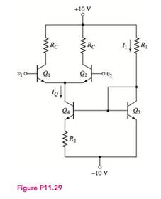
The transistor parameters for the circuit shown in Figure P 11.29 are
Want to see the full answer?
Check out a sample textbook solution
Chapter 11 Solutions
Microelectronics: Circuit Analysis and Design


- Class B Amplifier q1)If the input is 7.5Vp-p...DATA COLLECTION: What is the IL(peak)? a)7mA 6)mA 5)mA 4)mA q2) DATA COLLECTION: What is the Idc? a)3.84 b)4.82 c)3.82mA d)1.82mA q3)DATA COLLECTION: What is the input power in DC? Power input = 48.45mW Power input = 45.48mW Power input = 44.58mW Power input = 45.84mW q4) DATA COLLECTION: What is the output power in AC? a)18mW b)81mW c)11.8mW d)18.9mW q5)DATA COLLECTION: What is the power dissapated by each transistor? a)35.1mW b)53.1mW c)15.3mW d)13.5mW q6)DATA COLLECTION: What is the efficiency of class B amplifier? a)45% b)40% c)63% d)33% q7)arrow_forwardI think is true because the Wilson circuit provide a high output resistances , is it true or false and whyarrow_forwardQ1. The output characteristic of a typical transistor is shown below, where the quiescent point is selected on it. This transistor is used in the bias circuit presented below. Find the suitable values of Rg and Rc to fix the Q-point of the circuit properly. +Vcc = 12 V 12- Is = 70 uA 10- Ig = 60 uA 8- Rc Is = 50 uA Rs 6- Ig= 40 uA 4. Is = 30 uĄ Is = 20 uA B = 100 2- VBE = 0.7 V 0- -2- 2 4 6 8 10 12 14 16 VCE (V) Ic (mA)arrow_forward
- Instruction/s: Draw, Illustrate and label your schematic diagram before solving the problem.2.) Given a Collector -Feedback Biased transistor circuit with voltage at common collector is +10v ,base resistor is 100k ohms, Collector resistor is 10k ohms and Base current is 8.38 micro ampere, ,Voltage at Base-emitter junction is 0.7v. Determine Beta DC , Collector current and Voltage at collector-emitter junction. These might help as a guide to answer the problem...arrow_forwardSketch the de load line, quiescent collector current, quiescent voltsge, input power, output power and maximum efficiency of the circuit shown an Figure. The input results in a base current of 5 mA peak to peak What maximum output power can be delivered by the circuit, if the input voltage is changed resulting in a base current of 10mA peak to peak and hence find the maximum etficiency. cc=15 V R =18 2 -25arrow_forwardFigure 1(a) shows a series fed class A amplifier circuit. In order to achieve the maximum efficiency, the Q point must be located at the center of the DC load line as shown in Figure 1(b). This generates the maximum output current swing of Icmax (p – p) RC and the maximum output voltage swing is VCEmax(p – p) = Vcc Assume that the maximum input de power is (1 Vcc Pimax(dc) = Vcc!cQ(max)=Vcc \2° Rc. 2Rc Find the maximum efficiency, 7 of this circuit.arrow_forward
- Time left 1:46:17 A bipolar junction transistor is described in the figure below. The transistor is implemented in the circuit with Vcc, Rc, and RB equal to 16 volts, 2k, and 10kn. Determine the value of Vout if Vin = 1.1V. V... in RB B Vec Ro V E outarrow_forwardIn the circuit shown in Figure 1, the input signal vsig is a small sine-wave signal with zeroaverage. The transistor β is 100.Figure 1: BJT Amplifier(a) For RL = 10KΩ, draw the small-signal equivalent circuit of the amplifier and determineits overall voltage gain.(b) What is the input resistance of the amplifier circuit?arrow_forwardIt is connected to the input of a transistor (BJT) amplifier circuit with a gain of "-50" with a peak value of 100mV. a sine sign is applied a) Draw the circuit. b) Underline the input and output voltages by specifying their values.arrow_forward
- V* = + |ov Ri Rip ERC Vs RE V: -sV The following parameters are given for this transistor: B = 200 and VA = o. Design the circuit with the following value ICQ = 1.5mA and VCEQ = 5V. Find the small signal voltage gain AV = Vo/Vs. Find the input resistance in the signal source Vs.arrow_forwardCalculate the closed loop gain for the following circuit. Assume A = 0 for both transistors and R1+ R2 is very large. Circuit parameters / Devre Parametreleri 9m1 = 49 ms, 9m2 = 33 ms, R, = 101 kn, R2 = 26 k, Rp = 2.2 kn VDD Rp Vout ER Vino ER2 O a. 10.28 O b. 4.67 O c. 8.41 O d. 7.48 O e. 6.54 O f. 3.74 O g. 5.61 O h. 2.80 W WH. w-arrow_forwardQUESTION 10: The circuit parameters for diff-amp shown in Figure 11.30 are V* = 6 V, V = -6 V, and Io = 0.45 mA. The transistor parameters are ß = 74, V₁1 = V42 = 115 V₂ V 43 V 44 = 90 V, and V45 = ∞0. Determine the open-circuit differential-mode voltage gain. What is the output resistance of the diff-amp? Find the value of load resistance R₁ that reduces the differential-mode gain to 71 percent of the open-circuit value. Ad (open circuit) Format: 7842.2636277565 R₂ (kn) Format: 429.43075670268 Format: 672.96782467086 R₁ (kn) ibl iz i₁ 8mºd 2 V+ 25 V- i₂ = 8m'd 2 24 2₂ Signal ground V- Figure 11.30 Cc 8md 2 -Ove RL Sning Toolarrow_forward
 Introductory Circuit Analysis (13th Edition)Electrical EngineeringISBN:9780133923605Author:Robert L. BoylestadPublisher:PEARSON
 Delmar's Standard Textbook Of ElectricityElectrical EngineeringISBN:9781337900348Author:Stephen L. HermanPublisher:Cengage Learning
 Programmable Logic ControllersElectrical EngineeringISBN:9780073373843Author:Frank D. PetruzellaPublisher:McGraw-Hill Education
 Fundamentals of Electric CircuitsElectrical EngineeringISBN:9780078028229Author:Charles K Alexander, Matthew SadikuPublisher:McGraw-Hill Education
 Electric Circuits. (11th Edition)Electrical EngineeringISBN:9780134746968Author:James W. Nilsson, Susan RiedelPublisher:PEARSON
 Engineering ElectromagneticsElectrical EngineeringISBN:9780078028151Author:Hayt, William H. (william Hart), Jr, BUCK, John A.Publisher:Mcgraw-hill Education,