
Microelectronics: Circuit Analysis and Design
4th Edition
ISBN: 9780073380643
Author: Donald A. Neamen
Publisher: McGraw-Hill Companies, The
expand_more
expand_more
format_list_bulleted
Videos
Textbook Question
Chapter 11, Problem 11.67P
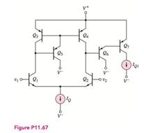
The diff-amp in Figure P 11.67 has a three-transistor active load circuit and a Darlington pair configuration connected to the output. Determine the bias current
Expert Solution & Answer
Want to see the full answer?
Check out a sample textbook solution
Students have asked these similar questions
Design a common-source amplifier (high gain) such that drain current is 11.33 Amp. State all the tech parameters and assumptions made.
Design a common-source amplifier such that gain is high and drain current is 11.33 amp. State the tech parameters and assumptions made.
QUESTION 12: The differential amplifier shown in Figure P11.60 has
a pair of pnp bipolars as input devices and a pair of npn bipolars
connected as an active load. The circuit is biased by Io=0.24 mA, and
the transistor parameters are ß = 80 , VẬP=90 V, and VAN = 115 V.
(a) Determine Io such that the de currents in the diff-amp are balanced.
(b) Find the open-circuit differential-mode voltage gain. (c) Determine
the differential-mode voltage gain if a load resistance R1 = 260 k2 is
connected to the output.
Io (HA)
Format : 4.595
Ad (open circuit)
Format : 4594.5
Ag (closed loop)
Format : 796.4
V+
Q2
Oa 어
RL
Q3
Q4
V-
Chapter 11 Solutions
Microelectronics: Circuit Analysis and Design
Ch. 11 - The circuit parameters for the differential...Ch. 11 - Consider the de transfer characteristics shown in...Ch. 11 - Prob. 11.1CSPCh. 11 - Consider the diff-amp described in Example 11.3 ....Ch. 11 - Prob. 11.4EPCh. 11 - Prob. 11.1TYUCh. 11 - Prob. 11.2TYUCh. 11 - Assume the differential-mode gain of a diff-amp is...Ch. 11 - Prob. 11.5EPCh. 11 - Consider the diff-amp shown in Figure 11.15 ....
Ch. 11 - Prob. 11.7EPCh. 11 - Prob. 11.4TYUCh. 11 - Prob. 11.5TYUCh. 11 - The parameters of the diff-amp shown in Figure...Ch. 11 - For the differential amplifier in Figure 11.20,...Ch. 11 - The parameters of the circuit shown in Figure...Ch. 11 - The circuit parameters of the diff-amp shown in...Ch. 11 - Consider the differential amplifier in Figure...Ch. 11 - The diff-amp in Figure 11.19 is biased at IQ=100A....Ch. 11 - Prob. 11.10TYUCh. 11 - The diff-amp circuit in Figure 11.30 is biased at...Ch. 11 - Prob. 11.11EPCh. 11 - Prob. 11.12EPCh. 11 - Prob. 11.11TYUCh. 11 - Prob. 11.12TYUCh. 11 - Redesign the circuit in Figure 11.30 using a...Ch. 11 - Prob. 11.14TYUCh. 11 - Prob. 11.15TYUCh. 11 - Prob. 11.16TYUCh. 11 - Prob. 11.17TYUCh. 11 - Consider the Darlington pair Q6 and Q7 in Figure...Ch. 11 - Prob. 11.14EPCh. 11 - Consider the Darlington pair and emitter-follower...Ch. 11 - Prob. 11.19TYUCh. 11 - Prob. 11.15EPCh. 11 - Consider the simple bipolar op-amp circuit in...Ch. 11 - Prob. 11.17EPCh. 11 - Define differential-mode and common-mode input...Ch. 11 - Prob. 2RQCh. 11 - From the dc transfer characteristics,...Ch. 11 - What is meant by matched transistors and why are...Ch. 11 - Prob. 5RQCh. 11 - Explain how a common-mode output signal is...Ch. 11 - Define the common-mode rejection ratio, CMRR. What...Ch. 11 - What design criteria will yield a large value of...Ch. 11 - Prob. 9RQCh. 11 - Define differential-mode and common-mode input...Ch. 11 - Sketch the de transfer characteristics of a MOSFET...Ch. 11 - Sketch and describe the advantages of a MOSFET...Ch. 11 - Prob. 13RQCh. 11 - Prob. 14RQCh. 11 - Describe the loading effects of connecting a...Ch. 11 - Prob. 16RQCh. 11 - Prob. 17RQCh. 11 - Prob. 18RQCh. 11 - (a) A differential-amplifier has a...Ch. 11 - Prob. 11.2PCh. 11 - Consider the differential amplifier shown in...Ch. 11 - Prob. 11.4PCh. 11 - Prob. D11.5PCh. 11 - The diff-amp in Figure 11.3 of the text has...Ch. 11 - The diff-amp configuration shown in Figure P11.7...Ch. 11 - Consider the circuit in Figure P11.8, with...Ch. 11 - The transistor parameters for the circuit in...Ch. 11 - Prob. 11.10PCh. 11 - Prob. 11.11PCh. 11 - The circuit and transistor parameters for the...Ch. 11 - Prob. 11.13PCh. 11 - Consider the differential amplifier shown in...Ch. 11 - Consider the circuit in Figure P11.15. The...Ch. 11 - Prob. 11.16PCh. 11 - Prob. 11.17PCh. 11 - For the diff-amp in Figure 11.2, determine the...Ch. 11 - Prob. 11.19PCh. 11 - Prob. D11.20PCh. 11 - Prob. 11.21PCh. 11 - The circuit parameters of the diff-amp shown in...Ch. 11 - Consider the circuit in Figure P11.23. Assume the...Ch. 11 - Prob. 11.24PCh. 11 - Consider the small-signal equivalent circuit of...Ch. 11 - Prob. D11.26PCh. 11 - Prob. 11.27PCh. 11 - A diff-amp is biased with a constant-current...Ch. 11 - The transistor parameters for the circuit shown in...Ch. 11 - Prob. D11.30PCh. 11 - For the differential amplifier in Figure P 11.31...Ch. 11 - Prob. 11.32PCh. 11 - Prob. 11.33PCh. 11 - Prob. 11.34PCh. 11 - Prob. 11.35PCh. 11 - Prob. 11.36PCh. 11 - Consider the normalized de transfer...Ch. 11 - Prob. 11.38PCh. 11 - Consider the circuit shown in Figure P 11.39 . The...Ch. 11 - Prob. 11.40PCh. 11 - Prob. 11.41PCh. 11 - Prob. 11.42PCh. 11 - Prob. 11.43PCh. 11 - Prob. D11.44PCh. 11 - Prob. D11.45PCh. 11 - Prob. 11.46PCh. 11 - Consider the circuit shown in Figure P 11.47 ....Ch. 11 - Prob. 11.48PCh. 11 - Prob. 11.49PCh. 11 - Prob. 11.50PCh. 11 - Consider the MOSFET diff-amp with the...Ch. 11 - Consider the bridge circuit and diff-amp described...Ch. 11 - Prob. D11.53PCh. 11 - Prob. 11.54PCh. 11 - Prob. 11.55PCh. 11 - Consider the JFET diff-amp shown in Figure P11.56....Ch. 11 - Prob. 11.57PCh. 11 - Prob. 11.58PCh. 11 - Prob. D11.59PCh. 11 - The differential amplifier shown in Figure P 11.60...Ch. 11 - Prob. 11.61PCh. 11 - Consider the diff-amp shown in Figure P 11.62 ....Ch. 11 - Prob. 11.63PCh. 11 - The differential amplifier in Figure P11.64 has a...Ch. 11 - Prob. 11.65PCh. 11 - Consider the diff-amp with active load in Figure...Ch. 11 - The diff-amp in Figure P 11.67 has a...Ch. 11 - Consider the diff-amp in Figure P11.68. The PMOS...Ch. 11 - Prob. 11.69PCh. 11 - Prob. 11.70PCh. 11 - Prob. D11.71PCh. 11 - Prob. D11.72PCh. 11 - An all-CMOS diff-amp, including the current source...Ch. 11 - Prob. D11.74PCh. 11 - Consider the fully cascoded diff-amp in Figure...Ch. 11 - Consider the diff-amp that was shown in Figure...Ch. 11 - Prob. 11.77PCh. 11 - Prob. 11.78PCh. 11 - Prob. 11.79PCh. 11 - Prob. 11.80PCh. 11 - Consider the BiCMOS diff-amp in Figure 11.44 ,...Ch. 11 - The BiCMOS circuit shown in Figure P11.82 is...Ch. 11 - Prob. 11.83PCh. 11 - Prob. 11.84PCh. 11 - For the circuit shown in Figure P11.85, determine...Ch. 11 - The output stage in the circuit shown in Figure P...Ch. 11 - Prob. 11.87PCh. 11 - Consider the circuit in Figure P11.88. The bias...Ch. 11 - Prob. 11.89PCh. 11 - Consider the multistage bipolar circuit in Figure...Ch. 11 - Prob. D11.91PCh. 11 - Prob. 11.92PCh. 11 - For the transistors in the circuit in Figure...Ch. 11 - Prob. 11.94PCh. 11 - Prob. 11.95PCh. 11 - Prob. 11.96PCh. 11 - Consider the diff-amp in Figure 11.55 . The...Ch. 11 - The transistor parameters for the circuit in...
Knowledge Booster


Learn more about
Need a deep-dive on the concept behind this application? Look no further. Learn more about this topic, electrical-engineering and related others by exploring similar questions and additional content below.Similar questions
- Q For the following specifications Vez 10V lc 5 mA Is-20 MA A.--9 Design an Emitter stabilized (cmitter feedback) Bias circuit and ensure that the Q-point in the middle ofr the DC load linc.arrow_forwardb) Refer to BJT cascade amplifier in Figure Q2, determine the de bias voltages and collector current for each stage.arrow_forwarda) Calculate the VA voltage value.b) Given the input voltage (Vin) waveformin the above Op-amp circuit, Vtl (low)and Vtu (high) hysteresis crossoverCalculate the voltages. c) At the Vtl and Vtu transitions of the Vo voltageCalculate the position changes.arrow_forward
- Sketch DC and ac equivalent circuits and theoretically Analyze DC and ac analysis of a Single Stage JFET Common-Source Amplifier Circuit a. DC Equivalent Circuit b. ac Equivalent Circuit C. DC Analysis d. ac Analysisarrow_forwardPLEASE NEED NOW For the amplifier circuit of the Figure shown below, calculate the voltage gain of each stage, the overall amplifier voltage gain and the output voltage.arrow_forward11.13 The i-v characteristic of an n-channel enhancement MOSFET is shown in Figure P11.13(a); a standard amplifier circuit based on the n-channel MOSFET is shown in Figure P11.13(b). Determine the quiescent current ino and drain-to-source voltage vs 2.0 I= 25°C 1.8 1.6 Vas10 V- -9V- 1.4 1.2 8V- 1.0 0.8 7V- 0.6 0.4 5 V= 0.2 3 V- 1.0 2.0 3.0 4.0 5.0 6.0 7.0 8.0 9.0 10 Drain-source voltage vps. V (a) Rp VGD VDD VGS Va Drain current ip, Aarrow_forward
- DC BIAS WITH VOLTAGE FEEDBACK CONFIGURATION QUESTIONS: What happen to the collector voltage, if the emitter resistor is removed and connect the emitter junction to the ground? What happen to the collector current of question number 1? Explain why?arrow_forwardGiven a non inverting op – amp below, If the normalize gain is 34, calculate the AVH in dB.arrow_forwardCalculate the collector current IC and the emitter collector voltage VCE of the amplifier shown in the figure and determine if it is in active region. shown in the figure and determine if it is in active region. Beta = 150.2. Calculate the input impedance Zi and output impedance Zo if ro = 7.5k.3. Calculate the voltage gain Av of the amplifier.arrow_forward
- . To design a bias circuit with an emitter feedback resistor, the voltage from emitter to ground is typically around one-tenth of the supply voltage. true O Falsearrow_forwardWhat type of biasing circuit using in the common source JFET amplifier?arrow_forward2. Discuss and compare (by equations) between the relative levels of stability for the following biasing circuits: i. the fixed-bias circuit, ii. the emitter-stabilized bias circuit, iii. the voltage-divider bias circuit, and iv. the voltage-feedback circuit.arrow_forward
arrow_back_ios
SEE MORE QUESTIONS
arrow_forward_ios
Recommended textbooks for you
 Introductory Circuit Analysis (13th Edition)Electrical EngineeringISBN:9780133923605Author:Robert L. BoylestadPublisher:PEARSON
 Delmar's Standard Textbook Of ElectricityElectrical EngineeringISBN:9781337900348Author:Stephen L. HermanPublisher:Cengage Learning
 Programmable Logic ControllersElectrical EngineeringISBN:9780073373843Author:Frank D. PetruzellaPublisher:McGraw-Hill Education
 Fundamentals of Electric CircuitsElectrical EngineeringISBN:9780078028229Author:Charles K Alexander, Matthew SadikuPublisher:McGraw-Hill Education
 Electric Circuits. (11th Edition)Electrical EngineeringISBN:9780134746968Author:James W. Nilsson, Susan RiedelPublisher:PEARSON
 Engineering ElectromagneticsElectrical EngineeringISBN:9780078028151Author:Hayt, William H. (william Hart), Jr, BUCK, John A.Publisher:Mcgraw-hill Education,
Introductory Circuit Analysis (13th Edition)
Electrical Engineering
ISBN:9780133923605
Author:Robert L. Boylestad
Publisher:PEARSON
Delmar's Standard Textbook Of Electricity
Electrical Engineering
ISBN:9781337900348
Author:Stephen L. Herman
Publisher:Cengage Learning
Programmable Logic Controllers
Electrical Engineering
ISBN:9780073373843
Author:Frank D. Petruzella
Publisher:McGraw-Hill Education
Fundamentals of Electric Circuits
Electrical Engineering
ISBN:9780078028229
Author:Charles K Alexander, Matthew Sadiku
Publisher:McGraw-Hill Education
Electric Circuits. (11th Edition)
Electrical Engineering
ISBN:9780134746968
Author:James W. Nilsson, Susan Riedel
Publisher:PEARSON
Engineering Electromagnetics
Electrical Engineering
ISBN:9780078028151
Author:Hayt, William H. (william Hart), Jr, BUCK, John A.
Publisher:Mcgraw-hill Education,
Diode Logic Gates - OR, NOR, AND, & NAND; Author: The Organic Chemistry Tutor;https://www.youtube.com/watch?v=9lqwSaIDm2g;License: Standard Youtube License