
Concept explainers
Videos
Consider the circuit in Figure P11.23. Assume the Early voltage of
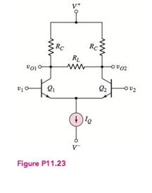
expressions for the one-sided differential-mode gain
Want to see the full answer?
Check out a sample textbook solution
Chapter 11 Solutions
Microelectronics: Circuit Analysis and Design


- A) Design with drawing an Op-Amp series voltage regulator to give a regulated O/P voltage of 12V for an I/P of 15V B) Calculate the line regulation if the I/p increases to 4V leads to increase the O/P voltage to 0.02V.arrow_forwardThe common-mode gain is . Select one: a. very high b. very low c. unpredictable d. always unityarrow_forwardFor the follower circuit in the figure below, consider k = 0.3x10⁻³ , rd = 100kOhm, VT = VGS(TH) = 3V and : (a) Draw the small-signal model considering the pi model (b) Determine the INPUT impedance (c) Determine the OUTPUT impedance (d) Determine the voltage gain (Av)arrow_forward
- Q2// Answer the following questions about voltage-feedback bias circuit for the figure below. 1-Determine Ver and VCB. 2- What happens to the voltage Ve if the resistor Rp is open? 22 K 3- What might cause VCE to become nearly 9 V? 4- Determine the change in Ie from 25° to 75° C, if Ico 0.2 HA, and VBE = 0.7V. 10 ul B-80arrow_forwardTwo single-stage capacitively coupled amplifiers like the one in the figure below are connected as a two-stage amplifier (RL is removed from the first stage). Determine whether or not this configuration will operate as a linear amplifier with an input voltage of 10 mV rms. If not, modify the design to achieve maximum gain without distortion. (provide modified design with explanation)arrow_forwardQ2. Order the output stages below based on their DC collector current. Use a descending order. +Vcc v+ VcC VB. Qn VBB RL Op i RL VCE Vcc (a) (b) (c) Concisely justify the answer.arrow_forward
- Adiff-amp is biased with a constant-current source lo- 0.25mA that has an output resistance of R. - 8MO. The bipolar transistor parameters are B=100, VT = 0.025 V and VA -. Determine the common-mode input resistance. O a. Ricm = 538 MA O b.Ricm- 308 MO OC Ricm = 808 MO Od Ricm = 704 MQarrow_forward11. i) Design a series Op-Amp regulated O/P of 12V which its I/P voltage is 20V. Chose the designed components and draw the circuit diagram ii) Design a shunt transistor regulated O/P of 6V which its I/P voltage is 15V. Chose the designed components and calculate I, with drawing the circuit diagramarrow_forwardsolve 4 Use a BJT op-amp)1 You’ve been asked to build an alarm system using monstable multvibrator having an activetime pf 100msec.. Explain the principle of operation and the type feedback of the op-amp.What is the advantage of this circuit?2 You’ve been asked to build a low frequency square wave generator using a basic comparatorhaving a frequency of 10kHz and 50% duty cycle. Explain the principle of operation and thetype of feedback of the op-amp. What is the advantage of this circuit?3 Build a Wein-Bridge oscillator using, C=1µF and +10V power supply to produce 10 kHzsinusoidal waveform. Generate your plots and compare output results. Highlight anydiscrepancies and discuss what happens if we want to increase the frequency to 100 kHz.4 Build a high frequency Colpitts oscillator producing 10kHz Discuss its advantage over RCoscillators. How can you modify the circuit to include a crystal in you circuit. What is atypical application of such an oscillator?arrow_forward
- The figure below shows a direct coupled two-stage amplifier. Determine. (i) d.c. voltages for both stages (VB1, VB2, Vc1, Vc2, VE1 and VE2. voltage gain of each stage and overall voltage gain.arrow_forwardThe transistor parameters for the circuit in Figure P11.9 are: B = 100, VBE (On) = 0.7 V, and VA = ∞o. (a) Determine RE such that IE = 150 μΑ. (b) Find Ad, Acm, and CMRRB for a one-sided output at vo2. (c) Determine the differential- and common-mode input resistances. Rc-50 k Rg = 0.5 kΩ www VI www 21 Figure P11.9 +10 V VOLVO2 IE RE -10 V ? Rc = 50 kΩ 22 Rg = 0.5 kΩ ww S'arrow_forwardQ5) Calculate the gain without and with feedback for the FET amplifier circuit with the following circuit values: R1 : = 100 kN, R2 : = 25 kN, Rp = 15 kN, RD = 12 kN + Cp Im = 4000 mS V. RL R2 ::arrow_forward
 Introductory Circuit Analysis (13th Edition)Electrical EngineeringISBN:9780133923605Author:Robert L. BoylestadPublisher:PEARSON
 Delmar's Standard Textbook Of ElectricityElectrical EngineeringISBN:9781337900348Author:Stephen L. HermanPublisher:Cengage Learning
 Programmable Logic ControllersElectrical EngineeringISBN:9780073373843Author:Frank D. PetruzellaPublisher:McGraw-Hill Education
 Fundamentals of Electric CircuitsElectrical EngineeringISBN:9780078028229Author:Charles K Alexander, Matthew SadikuPublisher:McGraw-Hill Education
 Electric Circuits. (11th Edition)Electrical EngineeringISBN:9780134746968Author:James W. Nilsson, Susan RiedelPublisher:PEARSON
 Engineering ElectromagneticsElectrical EngineeringISBN:9780078028151Author:Hayt, William H. (william Hart), Jr, BUCK, John A.Publisher:Mcgraw-hill Education,