
Videos
a.
The value of the resistor R1 and R2 in a way that the dc value of the output voltage is 0.
a.
Answer to Problem 11.89P
The value of the resistances are:
Explanation of Solution
Given:
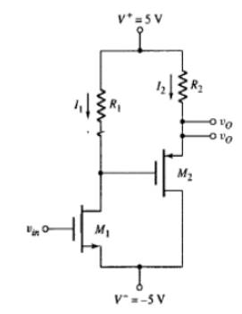
The circuit is given as:

The circuit parameters:
The drain current of
Considering the expression for drain current of
Hence, the value of the resistor
Evaluating the value of source gate voltage of
Considering the expression for the drain current of
Hence, the value of the resistor
b.
To sketch: The small signal equivalent circuit and then find the small signal transistor parameters.
b.
Explanation of Solution
Given:
The circuit is given as:

The circuit parameters:
Evaluating the value of trans-conductance
Substituting
Evaluating the value of trans-conductance of
Evaluating the value of the resistor
Evaluating the value of the resistor
c.
The small signal voltage gain.
c.
Answer to Problem 11.89P
The small signal gain of the circuit is -15.25V/V.
Explanation of Solution
Given:
The circuit is given as:
The circuit parameters:
Drawing the small signal equivalent model of the circuit:
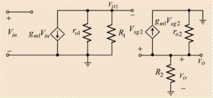
Applying nodal analysis at the input node:
Referring to the above diagram:
Applying the nodal analysis at the output node:
Hence, the small signal gain of the circuit is -15.25V/V.
d.
The output resistance.
d.
Answer to Problem 11.89P
The value of the output resistance is
Explanation of Solution
Given:
The circuit is given as:

The circuit parameters:
Evaluating the output resistance
Substituting
Hence, the value of the output resistance is
Want to see more full solutions like this?
Chapter 11 Solutions
Microelectronics: Circuit Analysis and Design


- FOLLOW UP QUESTIONS: BIPOLAR JUNCTION TRANSISTOR (BJT) SOLVE FOR: a.) VCE (off) CONSTRUCT A DC LINE SHOWING THE VALUES OF b.) IC (sat) c.) VCE (off) d.) ICQ e.) VCEQarrow_forwardDraw the DC circuit: b)DC computations: Compute the DC collector current of each transistor. I_C 1 = ________________________ mA I_C 2= ________________________ Calculations: c)Draw the AC circuit and compute gm, r_pi for the system. g_m 1= _______________________ mA/V r_pi 1 = _______________________ kohms g_m 2= _______________________ mA/V r_pi 2 = _______________________ kohms AC circuit: Calculations: d)Compute the gain A_v=Vo/Vi at the operational band (for sufficiently high frequency) Gain = A_v = ______________________________ Computations:arrow_forwardı just need the fınal answer Since Vcc = 20 V, RS = 3 kΩ, RB = 380 kΩ, RC = 1.2 kΩ, RE = 2.2 kΩ, RL = 911 Ω and β = 90 in the circuit in the figure, find the value of the output voltage (Vo). NOTE-1: It is within the 1 kHz mid-band frequency and the capacitors are negligible at this frequency. NOTE-2: The output impedance (r0) of the transistor will be neglected. a. 64,14 mV b. 83,88 mV c. 93,75 mV d. 74,01 mV e. 103,62 mV f. 24,67 mV g. 34,54 mV h. 49,34 mVarrow_forward
- *Proper Engineering Prefixes, (for micro use "u", example: 12.345 uA)*Strictly Three Decimal Places ONLY (example: 12.500 V)*FOR RESISTOR VALUES, Use Capital Letter "O", example: "123.456 kO" IMPORTANT: Do not round-off values in between calculations. ONLY THE FINAL ANSWER is rounded-off. Answer the ff: 1. What is the value of the base current? 2. What is the dc potential difference between the collector and emitter terminals? 3. What is the value of the input impedance? 4. What is the value of the output impedance? 5. What is the value of the voltage gain?arrow_forwardA CE Fixed Bias BJT configuration has the following parameters: Vcc=12V, Rb=220KOhms, Rc=2.2KOhms, Beta=30, ro=40KOhms. Determine hie. a.220 KOhms b.498.6 Ohms c.2.2 KOhms d.497.47 Ohmsarrow_forwardIn the circuit given below, Ra=Rb=Rc=9 ohm loads are fed with an AC voltage with a fundamental frequency of f=30Hz. The power value drawn from the source was measured as PK=5512.50 watts. Each switching element is triggered to be 120 degrees conduction. Calculate the effective values of the voltage Vab and the current flowing through the S1 switching element Vab_rms=, Ls1_rms?arrow_forward
- Since Vcc = 12 V, Vin = 690 mV, RB = 780 kΩ, RC1 = 27.9 Ω, RC2 = 25.4 Ω, RE = 470 Ω, RL = 47 Ω and β1 = β2 = 100 in the circuit in the figure Find the current (IL) flowing through RL? NOTE-1: VBE1 = VBE2 = 0.7 V will be taken. NOTE-2: Output impedances of transistors (r0) will be neglected. a. 16,56 mA b. 23,46 mA c. 8,28 mA d. 17,94 mA e. 20,70 mA f. 13,80 mA g. 26,22 mA h. 11,04 mAarrow_forwardIn the circuit given in the figure, what is the voltage gain (Av) of the circuit when = 100, r0 = 40 kΩ, RB = 360 kΩ, RC = 3.3 kΩ, RE = 220 Ω, Rs = 15 kΩ and RL = 166 kΩ?NOTE-1: The output impedance r0 of the transistor will be taken into the calculations.NOTE-2: Capacitors are negligible at mid-band frequency.arrow_forwardGiven: VCC = 20V RB = 390KΩ RC = 2.2KΩ RE = 1.2KΩ Beta = 80 rO = ∞ Calculate: a) re b) Zic) Z0d) AV e) Ai Transistor AC Analysis Bipolar Junction Transistor Repeat the problem in ACTIVITY 3 but with rO = 100 KΩarrow_forward
- Show the Common Emitter amplified output when sinusoidal 100Hz signal is applied at the input capacitor. Plz show the circuit diagramarrow_forwardR1 = 22 kohm and R2 = 220 kohm in the amplifiercircuit as shown. (a) What is the outputvoltage if vi = 0? (b) What is the output voltageif a dc signal VI = 0.22 V is applied to the circuit?(c) What is the output voltage if an ac signalvI = 0.15 sin 2500 πt V is applied to the circuit?(d) What is the output voltage if the input signal isvI = 0.22 − 0.15 sin 2500 πt V? (e) What is theinput current iI for parts (b), (c), and (d). (f) What isthe op amp output current iO for the input signals inparts (b), (c), and (d)? (g) What is the voltage at theinverting input of the op amp for the input signal inpart (d)?arrow_forwardDuring the turn-on and turn-off of a power transistor,the current-time and voltage-time relationshipsare as shown in the adjacent figure. Observe thewaveforms and calculate,1. The OFF-state power dissipation (static);2. The switch ON-state power dissipation(static);3. The average switching loss for the OFFtransition (dynamic);4. The average switching loss for the ONtransition (dynamic);Assume a switching frequency of 1kHz with Vx = 422Varrow_forward
 Introductory Circuit Analysis (13th Edition)Electrical EngineeringISBN:9780133923605Author:Robert L. BoylestadPublisher:PEARSON
 Delmar's Standard Textbook Of ElectricityElectrical EngineeringISBN:9781337900348Author:Stephen L. HermanPublisher:Cengage Learning
 Programmable Logic ControllersElectrical EngineeringISBN:9780073373843Author:Frank D. PetruzellaPublisher:McGraw-Hill Education
 Fundamentals of Electric CircuitsElectrical EngineeringISBN:9780078028229Author:Charles K Alexander, Matthew SadikuPublisher:McGraw-Hill Education
 Electric Circuits. (11th Edition)Electrical EngineeringISBN:9780134746968Author:James W. Nilsson, Susan RiedelPublisher:PEARSON
 Engineering ElectromagneticsElectrical EngineeringISBN:9780078028151Author:Hayt, William H. (william Hart), Jr, BUCK, John A.Publisher:Mcgraw-hill Education,