
Videos
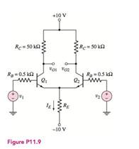
The transistor parameters for the circuit in Figure
Want to see the full answer?
Check out a sample textbook solution
Chapter 11 Solutions
Microelectronics: Circuit Analysis and Design


- For the op-amp shown, all transistors have B= 100, VBE = 0.7 V, and VA= 60 V. The %3D output resistance of all CCSS =0 and RL=1.2 kQ. A) Calculate the total gain. B) Calculate the maximum efficiency of the output stage for sinusoidal inputs. C) Redesign the circuit with a class AB output stage and calculate the maximum efficiency for the same load and CCSS? * +5 V 0. 2mA 1mA Ix V1a1 a2 v2 Q6 05 Vo Q3 2mA RL -5 Varrow_forwardA) Design with drawing an Op-Amp series voltage regulator to give a regulated O/P voltage of 12V for an I/P of 15V B) Calculate the line regulation if the I/p increases to 4V leads to increase the O/P voltage to 0.02V.arrow_forwardFigure 1(a) shows a series fed class A amplifier circuit. In order to achieve the maximum efficiency, the Q point must be located at the center of the DC load line as shown in Figure 1(b). This generates the maximum output current swing of Icmax (p – p) RC and the maximum output voltage swing is VCEmax(p – p) = Vcc Assume that the maximum input de power is (1 Vcc Pimax(dc) = Vcc!cQ(max)=Vcc \2° Rc. 2Rc Find the maximum efficiency, 7 of this circuit.arrow_forward
- I need the definitions of the following: •Open loop gain •Input resistance Ri •The output offset voltage (input offset voltage) •The output voltage swing (saturation voltage) •The bias current •The common mode rejection ratio CMRR Please, they can only be from the book "Franco, S. (2005). Design with Operational Amplifiers and Analogue Integrated Circuits.", "González, J. J. and Moreno, A. (2009). Applied Electronic Circuits with Amplifiers Operational", "Carter, B. and Mancini, R. (2009). Op Amps for Everyone" or also "Neamen, D. (2010). Microelectronics: Circuit Analysis and Design" Any of those pleasearrow_forwardClass B Amplifier q1)If the input is 7.5Vp-p...DATA COLLECTION: What is the IL(peak)? a)7mA 6)mA 5)mA 4)mA q2) DATA COLLECTION: What is the Idc? a)3.84 b)4.82 c)3.82mA d)1.82mA q3)DATA COLLECTION: What is the input power in DC? Power input = 48.45mW Power input = 45.48mW Power input = 44.58mW Power input = 45.84mW q4) DATA COLLECTION: What is the output power in AC? a)18mW b)81mW c)11.8mW d)18.9mW q5)DATA COLLECTION: What is the power dissapated by each transistor? a)35.1mW b)53.1mW c)15.3mW d)13.5mW q6)DATA COLLECTION: What is the efficiency of class B amplifier? a)45% b)40% c)63% d)33% q7)arrow_forward1. Without bypass capacitor CE, determine Av2. Without bypass capacitor CE, determine the current gainarrow_forward
- QUESTION 2: The differential amplifier in Figure P11.4 is biased with a three-transistor current source. The transistor parameters: B = 85 , VBE(on) = 0.7 V, and V= 0. Determine a new value of R1 such that VCE4 = 1.3 V. What are the values of Ic4, Ic2, and I4? Ic4 (mA) Format : 4.2 Ic2 (mA) Format : 8.382 I (mA) Format : 5.576 R1 (kN) Format : 5.969 +5 V 8.5 k2 2 k2 2 kQ Q4 VCE4 Qs Q3 Q2 VCE2 -5 V Figure P11.4 wwarrow_forwardQ2// Answer the following questions about voltage-feedback bias circuit for the figure below. 1-Determine Ver and VCB. 2- What happens to the voltage Ve if the resistor Rp is open? 22 K 3- What might cause VCE to become nearly 9 V? 4- Determine the change in Ie from 25° to 75° C, if Ico 0.2 HA, and VBE = 0.7V. 10 ul B-80arrow_forwardII.The following figure shows a class AB amplifier. (a) Determine the parameters of dc VB (Q1), VB (Q2), VE, ICQ, VCEQ (Q1), VCEQ (Q2). (b) For a 5-Vrms input, determine the power that is provided to the load resistor, and (c) Draw the output signal +Vcc +9 V 1.0kn D: R 5.0 V rms R2 10 kN -Vecarrow_forward
- Q2) Design a voltage-feedback bias circuit using a VCC supply of +10 V, and an npn silicon transistor with B of 100. Choose RC = 6RE=2RB and set IC at 2 mA and the stability factor S(ICO) at 3.arrow_forwardFor the follower circuit in the figure below, consider k = 0.3x10⁻³ , rd = 100kOhm, VT = VGS(TH) = 3V and : (a) Draw the small-signal model considering the pi model (b) Determine the INPUT impedance (c) Determine the OUTPUT impedance (d) Determine the voltage gain (Av)arrow_forward1) For a series regulator show that the output voltage can be made to be dependent only on a reference voltage and the feedback ratio. 2) list the 5 planar processes for Ic fabrication and explain them. 3) A circuit is built around a bi-polar NPN transistor. The base network has a diode and a capacitor in series while the collector is connected to the power supply through a resistor. if the resistor is connected to ground; i) draw the circuit ii) provide all the masking layout of the circuit 4) Explain the significance of the buried layer in npn transistor fabrication. 5) Draw the lateral view of the layout of a lateral pnp transistor. Label all the diffusion regions. 6) state five differences between series regulators and switching regulators.arrow_forward
 Introductory Circuit Analysis (13th Edition)Electrical EngineeringISBN:9780133923605Author:Robert L. BoylestadPublisher:PEARSON
 Delmar's Standard Textbook Of ElectricityElectrical EngineeringISBN:9781337900348Author:Stephen L. HermanPublisher:Cengage Learning
 Programmable Logic ControllersElectrical EngineeringISBN:9780073373843Author:Frank D. PetruzellaPublisher:McGraw-Hill Education
 Fundamentals of Electric CircuitsElectrical EngineeringISBN:9780078028229Author:Charles K Alexander, Matthew SadikuPublisher:McGraw-Hill Education
 Electric Circuits. (11th Edition)Electrical EngineeringISBN:9780134746968Author:James W. Nilsson, Susan RiedelPublisher:PEARSON
 Engineering ElectromagneticsElectrical EngineeringISBN:9780078028151Author:Hayt, William H. (william Hart), Jr, BUCK, John A.Publisher:Mcgraw-hill Education,