
Videos
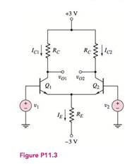
Consider the differential amplifier shown in Figure P 11.3 with transistor parameters
Want to see the full answer?
Check out a sample textbook solution
Chapter 11 Solutions
Microelectronics: Circuit Analysis and Design


- Correct the sentence: The aim of using coupling in multistage transistor amplifiers is to transfer DC output of one stage to the input of the next .stage and to isolate the d.c. conditions of one stage from the next stagearrow_forwardQ.4/ Refer to the class AB power amplifier shown below: a. Determine the de parameters VB(Q1), VB(Q2), Icq, VCEQ(QI), VcCEQ(Q2). b. For the 5Vrms input, determine the power delivered to the load resistor. c. Determine the approximate input resistance seen by the signal source if Bac=100. +Vcc +9 V 1.0 k2 D1 out D2 Q2 V. 5.0 V ms RL 50 Ω R2 1.0 k2 -Vcc -9 Varrow_forwardQ1. (a) Using the hybrid-pi model with early voltage effect, compute the small signal voltage gain, Av, input resistance and output resistance for the CE BJT amplifier shown below. Vec = 12 V B=100 VELON) = 0.7V V = 100V R = 93.7k2 %3D E R=6 kN Rg=0.5 k2 C, E R2= 6.3 k2 Figure Q1(a)arrow_forward
- Q.5/ Refer to the class AB amplifier in figure below operating with a single power supply: a. Find the de parameters VB(Q1), VB(Q2), VE, IcQ, VCEQ(QI), VCEQ(Q2). b. Assuming the input voltage is 10oVpp, calculate the power delivered to the load resistor. c. What faults causing the following troubles: 1. A positive half-wave output signal 2. OV on both bases and emitters 3. No output: emitter voltage =15V 4. Crossover distortion on the output. Vcc +15 V R 1.0 kN C3 C2 D2 Q2 RL V 75 N 1.0 kNarrow_forwardClass B Amplifier q1)If the input is 7.5Vp-p...DATA COLLECTION: What is the IL(peak)? a)7mA 6)mA 5)mA 4)mA q2) DATA COLLECTION: What is the Idc? a)3.84 b)4.82 c)3.82mA d)1.82mA q3)DATA COLLECTION: What is the input power in DC? Power input = 48.45mW Power input = 45.48mW Power input = 44.58mW Power input = 45.84mW q4) DATA COLLECTION: What is the output power in AC? a)18mW b)81mW c)11.8mW d)18.9mW q5)DATA COLLECTION: What is the power dissapated by each transistor? a)35.1mW b)53.1mW c)15.3mW d)13.5mW q6)DATA COLLECTION: What is the efficiency of class B amplifier? a)45% b)40% c)63% d)33% q7)arrow_forwardQ) One of the advantages of a Direct-coupled amplifier is ..... ... (a) Thermal instability (b) Constant gain from zero (dc) to high frequency (c) Small size (d) Low costarrow_forward
- 5, a) Determine Vdsat when ID=.5 mA. b) Determine Kn when ID = 0.5 Amps. (Show your work!) c) Determine VTN. (Show your work!) d) Vgs Consider the circuit and corresponding graph, shown below. ID (mA) 0.60 0.50 0.40 0.30 0.20 0.10 0.00 0 0.5 Vds 1 1.5 2 2.5 Vds 3 3.5 4 4.5 5 -Vgs = 1V - Vgs = 1.1V - Vgs = 1.2V - Vgs = 1.3Varrow_forward(a) Using the hybrid-pi model with early voltage effect, compute the small signal voltage gain, Av, input resistance and output resistance for the CE BJT amplifier shown below. Q1. Vcc = 12 V B=100 VBE(ON) = 0.7V V = 100V R = 93.7k2 * R=6 k2 Vo Rs = 0.5 k2 C B E R,= 6.3 k2 Figure Q1(a)arrow_forwardGiven a D-MOSFET circuit used as an amplifier with the following parameter: IDSS=12mA and a transconductance of gm=3.2 mS. Determine the DC drain to source voltage VDS and the AC output voltage if Vin=500 mV.arrow_forward
- The amplifier in the circuit below is driven by a signal generator v, with a small sine wave signal vhose average value is zero. Assume the transistor has a value of B-100, and V-26 mV. a. You need to design the circuit so that the de emitter current IE of the emitter resistor RE to establish the desired de emitter current. = 1 mA. Specify the value b. A de collector voltage of +5 volts is desired. Specify the value of the collector resistor Re to establish the desired de collector voltage. For this part assume that RL 5 K and the Early Effect needs to be considered. The transistor has a VA 100 Volts. Draw the ac small signal equivalent circuit model of the amplifier and determine its voltage gain. 91SV C. 2.5k MM do RE -15 V 84 Vout RLarrow_forwardInstruction/s: Draw, Illustrate and label your schematic diagram before solving the problem.2.) Given a Collector -Feedback Biased transistor circuit with voltage at common collector is +10v ,base resistor is 100k ohms, Collector resistor is 10k ohms and Base current is 8.38 micro ampere, ,Voltage at Base-emitter junction is 0.7v. Determine Beta DC , Collector current and Voltage at collector-emitter junction. These might help as a guide to answer the problem...arrow_forwardQ1. (a) Consider the amplifier circuit in Figure Q1(a). Given the following: RI = 100 k2 R2 = 56 kN Rc =2 k2 Vcc = +8 V Assume the transistor has B = 100 and VBE(on) = 0.7 V. You may neglect Early effect and use VT = 26 mV. (i) Draw the DC equivalent circuit, then determine Iç and VCE. Draw the AC equivalent circuit using re model. Based on this, determine the parameters Av, Rin and Rout. (ii) Vcc Rc R1 R2 C3 Vout C2 Ci Vin Figure Q1(a)arrow_forward
 Introductory Circuit Analysis (13th Edition)Electrical EngineeringISBN:9780133923605Author:Robert L. BoylestadPublisher:PEARSON
 Delmar's Standard Textbook Of ElectricityElectrical EngineeringISBN:9781337900348Author:Stephen L. HermanPublisher:Cengage Learning
 Programmable Logic ControllersElectrical EngineeringISBN:9780073373843Author:Frank D. PetruzellaPublisher:McGraw-Hill Education
 Fundamentals of Electric CircuitsElectrical EngineeringISBN:9780078028229Author:Charles K Alexander, Matthew SadikuPublisher:McGraw-Hill Education
 Electric Circuits. (11th Edition)Electrical EngineeringISBN:9780134746968Author:James W. Nilsson, Susan RiedelPublisher:PEARSON
 Engineering ElectromagneticsElectrical EngineeringISBN:9780078028151Author:Hayt, William H. (william Hart), Jr, BUCK, John A.Publisher:Mcgraw-hill Education,