
Videos
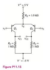
Consider the circuit in Figure P11.15. The transistor parameters are
Want to see the full answer?
Check out a sample textbook solution
Chapter 11 Solutions
Microelectronics: Circuit Analysis and Design


- Open with v Consider class-A emitter follower circuit shown in the figure below. The circuit parameters are V+ = 24 V, V- = -24 V, and RL = 2000. The transistor parameters are B = 50, VBElon) = 0.7 V, and VCElsat) = 0.2 V. The output voltage is to vary between +20 V and -20 V. The minimum current in Q1 is to be ie1 = 20 mA. For vo = 0, find the power dissipated in the first transistor Q1- V+arrow_forwardQUESTION 5: Consider the differential amplifier in Figure P11.17 with parameters V = 5 V, V = -5 V, and Io = 0.8 mA. Neglect base currents and assume V₁ = ∞ for all transistors. The emitter currents can be written as I£1 = IS1 EXP(VBE1/VT) and I£2 = 152 EXP(VBE2/VT). If v₁ = v₂ = 0, Is1 = 2.3 x 10-¹5 A and Is2 = 2.2 x 10-¹5 A, determine (v01 - v0₂) for Rc₁ = 7.2 k and Rc2 = 7.9 kq. IE1 (mA) Format : 0.3093 IE2 (mA) Format : 0.5634 (V01 - V02) (V) Format: 0.5862 V+ R₁ 2₁ Rc1 VOI Rc2 O V02 2₂ V Figure P11.17 V₂ 24arrow_forwardThe transistor parameters for the circuit in Figure P11.9 are: B = 100, VBE (On) = 0.7 V, and VA = ∞o. (a) Determine RE such that IE = 150 μΑ. (b) Find Ad, Acm, and CMRRB for a one-sided output at vo2. (c) Determine the differential- and common-mode input resistances. Rc-50 k Rg = 0.5 kΩ www VI www 21 Figure P11.9 +10 V VOLVO2 IE RE -10 V ? Rc = 50 kΩ 22 Rg = 0.5 kΩ ww S'arrow_forward
- Instruction/s: Draw, Illustrate and label your schematic diagram before solving the problem. 1.) Given a Fixed-Biased transistor circuit with Beta DC is 200 , voltage at common collector is +22v ,base supply voltage is +11V, Base resistor is 47kOhms , collector resistor is 390 ohms ,Voltage at Base-emitter junction is 0.7v. Determine the Q-point of collector current and Voltage at collector-emitter junction. These is the example or guide that might help in answering the problem.arrow_forwarda) The n-channel JFET and the D-MOSFET have very similar I-V output characteristics. Which of these two structures can be operated in enhancement mode and why is that possible?arrow_forward(ii) Calculate the RB, Rc, and the minimum power rating of the transistor (Note: the actual power rating should be greater).arrow_forward
- QUESTION 5: A simplified class-AB output stage with BJTS is shown below. The circuit parameters are Vcc=15 V and R1 = 1900 2. For each transistor, Is= 9 x 10 ¬15 A. Determine the value of VBg that produces icn =ico=1 mA when vị= 0. What is the power dissipated in each transistor? Format : 2.7987275900068 VBB (V) Format : 62 Pon (mW)| (mW)| Format : 26 +Vcc icn VBB V BB 2 RL Qp lice -Vcc wwarrow_forwardQUESTION 1: The differential amplifier in Figure P11.4 is biased with a three-transistor current source. The transistor parameters: B = 160 , VBE(on) = 0.68 V, and V= 0. Determine I1, Ic2» Ic4, V CE2, and V CE4• 1 (mA) Format : 8.0238 Ic2 (mA) Ic4 (mA) Format : 8.0929 Format : 0.207 VCE2 (V) Format : 5.98 V CE4 (V) Format : 7.2693 +5 V R = 8.5 k2 Rc = 2 k2 2 k2 ICA Q4 VCE4 Q5 Q3 Q2 VCE2 -5 V Figure P11.4arrow_forwardWhat is the preferred D-MOSFET biasing method? O a. Drain-to-source voltage is zero O b. VGS= 0. O c. Apply source voltage to gate O d. Hold gate-to-source at AC input levelsarrow_forward
- 26 Determine Vị and I, for the two-stage amplifier shown in the circult of Figure P11.26, with identical MOSFETS having K =1 A/V? and Vr =3V, for a. VG = 4 V, b. VG = 5 V c. VG = 4+0.1 cos(750) %3Darrow_forwardHow do you determine when a transistor is in cutoff? A when VE = 0 v B) when VCE = Vcc C) when VCE = Vcc / 2 D when Ic = maximumarrow_forwardQUESTION 2: The differential amplifier in Figure P11.4 is biased with a three-transistor current source. The transistor parameters: B = 85 , VBE(on) = 0.7 V, and V= 0. Determine a new value of R1 such that VCE4 = 1.3 V. What are the values of Ic4, Ic2, and I4? Ic4 (mA) Format : 4.2 Ic2 (mA) Format : 8.382 I (mA) Format : 5.576 R1 (kN) Format : 5.969 +5 V 8.5 k2 2 k2 2 kQ Q4 VCE4 Qs Q3 Q2 VCE2 -5 V Figure P11.4 wwarrow_forward
 Introductory Circuit Analysis (13th Edition)Electrical EngineeringISBN:9780133923605Author:Robert L. BoylestadPublisher:PEARSON
 Delmar's Standard Textbook Of ElectricityElectrical EngineeringISBN:9781337900348Author:Stephen L. HermanPublisher:Cengage Learning
 Programmable Logic ControllersElectrical EngineeringISBN:9780073373843Author:Frank D. PetruzellaPublisher:McGraw-Hill Education
 Fundamentals of Electric CircuitsElectrical EngineeringISBN:9780078028229Author:Charles K Alexander, Matthew SadikuPublisher:McGraw-Hill Education
 Electric Circuits. (11th Edition)Electrical EngineeringISBN:9780134746968Author:James W. Nilsson, Susan RiedelPublisher:PEARSON
 Engineering ElectromagneticsElectrical EngineeringISBN:9780078028151Author:Hayt, William H. (william Hart), Jr, BUCK, John A.Publisher:Mcgraw-hill Education,