
Videos
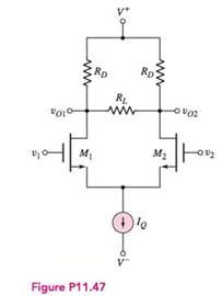
Consider the circuit shown in Figure P 11.47 . Assume that
Want to see the full answer?
Check out a sample textbook solution
Chapter 11 Solutions
Microelectronics: Circuit Analysis and Design


- Q2) for the amplifier shown in Figure 1) Determine the voltage gain (Av) and the current Gain (Ai) 2) Determine The input and output resistance 3) Determine The output voltage Vout 4) Draw The Ac load line 5) Draw the AC equivalent circuit 6) Determine the maximum input voltage (Vi(p-p)) for maximum output voltage (Vo(p-p)) without distortion. HH Vi-20 mv RB 56 kQ +₁ D B = 50 - 10 V HH RE 1kQ Vou RL • 10 Ω ww11arrow_forwardThe term duty cycle refers to the amount of time a signal is complete cycle. A. off compared to the period of one B. on The output voltage of op-amp is positive saturation, when the voltage applied to the input is greater than the input. A. inverting B. noninverting A square wave that is 20V at its high state and OV when it is off will produce an average DC when its duty cycle is 75%. Formula: VOUT = Duty Cycle * Peak voltage voltage of A. 7.5V B. 10V C. 15Varrow_forwardQ2// Answer the following questions about voltage-feedback bias circuit for the figure below. 1-Determine Ver and VCB. 2- What happens to the voltage Ve if the resistor Rp is open? 22 K 3- What might cause VCE to become nearly 9 V? 4- Determine the change in Ie from 25° to 75° C, if Ico 0.2 HA, and VBE = 0.7V. 10 ul B-80arrow_forward
- 1) For a series regulator show that the output voltage can be made to be dependent only on a reference voltage and the feedback ratio. 2) list the 5 planar processes for Ic fabrication and explain them. 3) A circuit is built around a bi-polar NPN transistor. The base network has a diode and a capacitor in series while the collector is connected to the power supply through a resistor. if the resistor is connected to ground; i) draw the circuit ii) provide all the masking layout of the circuit 4) Explain the significance of the buried layer in npn transistor fabrication. 5) Draw the lateral view of the layout of a lateral pnp transistor. Label all the diffusion regions. 6) state five differences between series regulators and switching regulators.arrow_forwardQ2) Design a voltage-feedback bias circuit using a VCC supply of +10 V, and an npn silicon transistor with B of 100. Choose RC = 6RE=2RB and set IC at 2 mA and the stability factor S(ICO) at 3.arrow_forward11. i) Design a series Op-Amp regulated O/P of 12V which its I/P voltage is 20V. Chose the designed components and draw the circuit diagram ii) Design a shunt transistor regulated O/P of 6V which its I/P voltage is 15V. Chose the designed components and calculate I, with drawing the circuit diagramarrow_forward
- The common-mode gain is . Select one: a. very high b. very low c. unpredictable d. always unityarrow_forwardC. A variable capacitor. O d. An amplifier. When operating in the saturation region, the current gain 'B' of the bipolar transistor increases Select one: OTrue O False Assume Is= 8x 10⁵ A, B-100, and VA =-. For the circuit shown below and for -0.5 mA, the value of the transconduce Vcc=2 V Q1arrow_forwardAnswer the following with illustration and solutions. 2.) If C1 = C2 = 100pF, determine the output frequencies produced by this arrangement:a. (a) when R1 = R2 = 12kilo-ohms andb. (b) when R1 = R2 = 8kilo-ohms See the example below..arrow_forward
- Introducion to Electronic Analysis and Design - CE05 To have a good amplifier Select one: a. The input resistance should be high b. the output resistance should be high c. the voltage gain should be equal to zero d. the current gain should be equal to zero Ssment CE255/EE255 (O1)- Dr. Mamoun Al-Mistar Jump to...arrow_forwardand Rc parameters: VBE places. Given the PNP differential amplifier circuit below with Vcc 3.3k, answer the following questions. Note that -0.7V, VCE,SAT -0.2V, V₁ → ∞, and V1 - Ici = 1. What are the DC collector currents? Ic₂ C1 mA mA = EE TAIL = C2 5V, VEE = -5V, ITAIL 1mA, V₁ = V₂ = 0v, ₁ and 2 are matched and has the following →∞. Express your answers in 2 decimal V2 =arrow_forward6.) A differential amplifier has a differential voltage gain of 2000 and a common mode gain of 0.2. What is the common mode rejection ratio in dB?arrow_forward
 Introductory Circuit Analysis (13th Edition)Electrical EngineeringISBN:9780133923605Author:Robert L. BoylestadPublisher:PEARSON
 Delmar's Standard Textbook Of ElectricityElectrical EngineeringISBN:9781337900348Author:Stephen L. HermanPublisher:Cengage Learning
 Programmable Logic ControllersElectrical EngineeringISBN:9780073373843Author:Frank D. PetruzellaPublisher:McGraw-Hill Education
 Fundamentals of Electric CircuitsElectrical EngineeringISBN:9780078028229Author:Charles K Alexander, Matthew SadikuPublisher:McGraw-Hill Education
 Electric Circuits. (11th Edition)Electrical EngineeringISBN:9780134746968Author:James W. Nilsson, Susan RiedelPublisher:PEARSON
 Engineering ElectromagneticsElectrical EngineeringISBN:9780078028151Author:Hayt, William H. (william Hart), Jr, BUCK, John A.Publisher:Mcgraw-hill Education,