
Videos
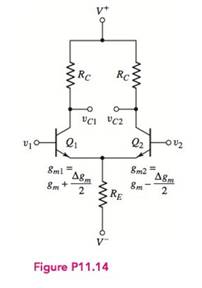
Consider the differential amplifier shown in Figure P11.14 with mismatched transistors. The mismatched transistors result in mismatched transconductances as shown. The circuit and transistor parameters are
Want to see the full answer?
Check out a sample textbook solution
Chapter 11 Solutions
Microelectronics: Circuit Analysis and Design


- Class B Amplifier q1)If the input is 7.5Vp-p...DATA COLLECTION: What is the IL(peak)? a)7mA 6)mA 5)mA 4)mA q2) DATA COLLECTION: What is the Idc? a)3.84 b)4.82 c)3.82mA d)1.82mA q3)DATA COLLECTION: What is the input power in DC? Power input = 48.45mW Power input = 45.48mW Power input = 44.58mW Power input = 45.84mW q4) DATA COLLECTION: What is the output power in AC? a)18mW b)81mW c)11.8mW d)18.9mW q5)DATA COLLECTION: What is the power dissapated by each transistor? a)35.1mW b)53.1mW c)15.3mW d)13.5mW q6)DATA COLLECTION: What is the efficiency of class B amplifier? a)45% b)40% c)63% d)33% q7)arrow_forwardFor the op-amp shown, all transistors have B= 100, VBE = 0.7 V, and VA= 60 V. The %3D output resistance of all CCSS =0 and RL=1.2 kQ. A) Calculate the total gain. B) Calculate the maximum efficiency of the output stage for sinusoidal inputs. C) Redesign the circuit with a class AB output stage and calculate the maximum efficiency for the same load and CCSS? * +5 V 0. 2mA 1mA Ix V1a1 a2 v2 Q6 05 Vo Q3 2mA RL -5 Varrow_forwardQUESTION 2: The differential amplifier in Figure P11.4 is biased with a three-transistor current source. The transistor parameters: B = 85 , VBE(on) = 0.7 V, and V= 0. Determine a new value of R1 such that VCE4 = 1.3 V. What are the values of Ic4, Ic2, and I4? Ic4 (mA) Format : 4.2 Ic2 (mA) Format : 8.382 I (mA) Format : 5.576 R1 (kN) Format : 5.969 +5 V 8.5 k2 2 k2 2 kQ Q4 VCE4 Qs Q3 Q2 VCE2 -5 V Figure P11.4 wwarrow_forward
- The common-mode gain is ........... 1. very high 2. very low 3. always unity 4. unpredictablearrow_forwardDesign an Inverting Summing amplifier to add 0.1 Volt, 0.2 Volt and 0.3 Volt. Vo should be obtained as 6 V. Draw the circuit diagram and derive the expression as wellIarrow_forwardDraw the DC and AC load line for a transistor amplifier circuit shown in Figure, also describe the optimum operating Point for the given values as follows: Rc = 10 KQ ; RL=20 KQ and V cc = 20 V +Vcc Ic Rc Cc Cc V. out R1 Vin wwwarrow_forward
- I think is true because the Wilson circuit provide a high output resistances , is it true or false and whyarrow_forwardC. A variable capacitor. O d. An amplifier. When operating in the saturation region, the current gain 'B' of the bipolar transistor increases Select one: OTrue O False Assume Is= 8x 10⁵ A, B-100, and VA =-. For the circuit shown below and for -0.5 mA, the value of the transconduce Vcc=2 V Q1arrow_forwardWhich is the correct expression for Vo (the quiescent output voltage) for the circuit shown here (you can assume that the transistor has a large-signal current gain of hFE>>1)? (Symbols have their usual meaning, with / and V being quiescent currents and voltages, and i and v being small signal values) -Vcc R1 R2 Vo=Vcc 0 Vo = Vec- Vo=Vcc - Q1 - RL - Cin RE Vcc R₂ |V₁ = Vcc - R₁ + R₂ Vo -Vo+vo -vi RL Vcc R₂ RE R₁ + R₂ - R₁ Vcc RL R₂ R₁ + RE R₁ VccR₂ RE 0.7 -0.7] − −0.7] R₁ + R₂arrow_forward
- 6. This problem involves designing a differential amplifier of the following figure. You may assume that the body and source terminal is shorted and you can neglect channel length modulation. Use the following MOSFET parameters: Parameter N-channel P-channel Units +1.10 -1.20 V 5. 2E-5 A/v 1.5E-5 a) Choose IBIAS for an output DC bias level Vo1(Dc) = Voz(DC)=3.00 V. b) Determine the voltage gain of the differential amplifier. c) Determine the magnitude of the small signal common mode gain. VDD = +5V RD1 5kQ RD2 5kO Voi0 o Vo2 M1 M2 W/L=80/2 w/L=80/2 ) IBIAS Vss = -5Varrow_forwardCalculate the common-mode gain for the amplifier circuit below. Refer to the image for the circuit configuration, but refer to the following for the values: Vcc = 10 V, Rc = 74674 ohms, RE = 70254 ohms, -Vcc = -11 V, Vi1 = 0 V, ri1=ri2= 29354 ohms, beta1=beta2 = 75.arrow_forwardQUESTION 12: The differential amplifier shown in Figure P11.60 has a pair of pnp bipolars as input devices and a pair of npn bipolars connected as an active load. The circuit is biased by Io=0.24 mA, and the transistor parameters are ß = 80 , VẬP=90 V, and VAN = 115 V. (a) Determine Io such that the de currents in the diff-amp are balanced. (b) Find the open-circuit differential-mode voltage gain. (c) Determine the differential-mode voltage gain if a load resistance R1 = 260 k2 is connected to the output. Io (HA) Format : 4.595 Ad (open circuit) Format : 4594.5 Ag (closed loop) Format : 796.4 V+ Q2 Oa 어 RL Q3 Q4 V-arrow_forward
 Introductory Circuit Analysis (13th Edition)Electrical EngineeringISBN:9780133923605Author:Robert L. BoylestadPublisher:PEARSON
 Delmar's Standard Textbook Of ElectricityElectrical EngineeringISBN:9781337900348Author:Stephen L. HermanPublisher:Cengage Learning
 Programmable Logic ControllersElectrical EngineeringISBN:9780073373843Author:Frank D. PetruzellaPublisher:McGraw-Hill Education
 Fundamentals of Electric CircuitsElectrical EngineeringISBN:9780078028229Author:Charles K Alexander, Matthew SadikuPublisher:McGraw-Hill Education
 Electric Circuits. (11th Edition)Electrical EngineeringISBN:9780134746968Author:James W. Nilsson, Susan RiedelPublisher:PEARSON
 Engineering ElectromagneticsElectrical EngineeringISBN:9780078028151Author:Hayt, William H. (william Hart), Jr, BUCK, John A.Publisher:Mcgraw-hill Education,