
Microelectronics: Circuit Analysis and Design
4th Edition
ISBN: 9780073380643
Author: Donald A. Neamen
Publisher: McGraw-Hill Companies, The
expand_more
expand_more
format_list_bulleted
Videos
Textbook Question
Chapter 11, Problem 11.8P
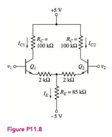
Consider the circuit in Figure P11.8, with transistor parameters: β=100 VBE(on)=0.7V, and VA=∞. (a) For v1=v2=0, find IC1,IC2,IE,VCE1 and VCE2 (b) Determine the maximum and minimum values of the common-mode input voltage. (c) Calculate Ad for a one-sided output at the collector of Q2 .
Expert Solution & Answer
Want to see the full answer?
Check out a sample textbook solution
Students have asked these similar questions
Exam2
Subject: (Numerical Analysis)
Class: Third
Date: 27/4/2025
Time: 60 minutes
Q1. For what values of k does this system of equations has no solution? (use Gauss-Jordan eliminations)
kx + y + z = 1
x+ky + z = 1
x+y+kz=1
Consider the Difference equation of a causal Linear time-invariant (LTI) system given
by: (y(n) - 1.5y(n - 1) + 0.5y(n = 2) = x(n)
a) Implement the difference equation model of this system.
b) Find the system transfer function H(z).
c) For an input x(n) = 8(n), determine the output response y(n).
d) Verify the initial value theorem y(0) with part (c).
Q5B. Find the type of the controller in the following figures and use real values to find the transfer
function of three of them[ Hint Pi,Pd and Lead,lag are found so put the controller with its
corresponding compensator].
R₁
R₂
Rz
HE
C2
RA
HE
R₁
R2
RA
と
Chapter 11 Solutions
Microelectronics: Circuit Analysis and Design
Ch. 11 - The circuit parameters for the differential...Ch. 11 - Consider the de transfer characteristics shown in...Ch. 11 - Prob. 11.1CSPCh. 11 - Consider the diff-amp described in Example 11.3 ....Ch. 11 - Prob. 11.4EPCh. 11 - Prob. 11.1TYUCh. 11 - Prob. 11.2TYUCh. 11 - Assume the differential-mode gain of a diff-amp is...Ch. 11 - Prob. 11.5EPCh. 11 - Consider the diff-amp shown in Figure 11.15 ....
Ch. 11 - Prob. 11.7EPCh. 11 - Prob. 11.4TYUCh. 11 - Prob. 11.5TYUCh. 11 - The parameters of the diff-amp shown in Figure...Ch. 11 - For the differential amplifier in Figure 11.20,...Ch. 11 - The parameters of the circuit shown in Figure...Ch. 11 - The circuit parameters of the diff-amp shown in...Ch. 11 - Consider the differential amplifier in Figure...Ch. 11 - The diff-amp in Figure 11.19 is biased at IQ=100A....Ch. 11 - Prob. 11.10TYUCh. 11 - The diff-amp circuit in Figure 11.30 is biased at...Ch. 11 - Prob. 11.11EPCh. 11 - Prob. 11.12EPCh. 11 - Prob. 11.11TYUCh. 11 - Prob. 11.12TYUCh. 11 - Redesign the circuit in Figure 11.30 using a...Ch. 11 - Prob. 11.14TYUCh. 11 - Prob. 11.15TYUCh. 11 - Prob. 11.16TYUCh. 11 - Prob. 11.17TYUCh. 11 - Consider the Darlington pair Q6 and Q7 in Figure...Ch. 11 - Prob. 11.14EPCh. 11 - Consider the Darlington pair and emitter-follower...Ch. 11 - Prob. 11.19TYUCh. 11 - Prob. 11.15EPCh. 11 - Consider the simple bipolar op-amp circuit in...Ch. 11 - Prob. 11.17EPCh. 11 - Define differential-mode and common-mode input...Ch. 11 - Prob. 2RQCh. 11 - From the dc transfer characteristics,...Ch. 11 - What is meant by matched transistors and why are...Ch. 11 - Prob. 5RQCh. 11 - Explain how a common-mode output signal is...Ch. 11 - Define the common-mode rejection ratio, CMRR. What...Ch. 11 - What design criteria will yield a large value of...Ch. 11 - Prob. 9RQCh. 11 - Define differential-mode and common-mode input...Ch. 11 - Sketch the de transfer characteristics of a MOSFET...Ch. 11 - Sketch and describe the advantages of a MOSFET...Ch. 11 - Prob. 13RQCh. 11 - Prob. 14RQCh. 11 - Describe the loading effects of connecting a...Ch. 11 - Prob. 16RQCh. 11 - Prob. 17RQCh. 11 - Prob. 18RQCh. 11 - (a) A differential-amplifier has a...Ch. 11 - Prob. 11.2PCh. 11 - Consider the differential amplifier shown in...Ch. 11 - Prob. 11.4PCh. 11 - Prob. D11.5PCh. 11 - The diff-amp in Figure 11.3 of the text has...Ch. 11 - The diff-amp configuration shown in Figure P11.7...Ch. 11 - Consider the circuit in Figure P11.8, with...Ch. 11 - The transistor parameters for the circuit in...Ch. 11 - Prob. 11.10PCh. 11 - Prob. 11.11PCh. 11 - The circuit and transistor parameters for the...Ch. 11 - Prob. 11.13PCh. 11 - Consider the differential amplifier shown in...Ch. 11 - Consider the circuit in Figure P11.15. The...Ch. 11 - Prob. 11.16PCh. 11 - Prob. 11.17PCh. 11 - For the diff-amp in Figure 11.2, determine the...Ch. 11 - Prob. 11.19PCh. 11 - Prob. D11.20PCh. 11 - Prob. 11.21PCh. 11 - The circuit parameters of the diff-amp shown in...Ch. 11 - Consider the circuit in Figure P11.23. Assume the...Ch. 11 - Prob. 11.24PCh. 11 - Consider the small-signal equivalent circuit of...Ch. 11 - Prob. D11.26PCh. 11 - Prob. 11.27PCh. 11 - A diff-amp is biased with a constant-current...Ch. 11 - The transistor parameters for the circuit shown in...Ch. 11 - Prob. D11.30PCh. 11 - For the differential amplifier in Figure P 11.31...Ch. 11 - Prob. 11.32PCh. 11 - Prob. 11.33PCh. 11 - Prob. 11.34PCh. 11 - Prob. 11.35PCh. 11 - Prob. 11.36PCh. 11 - Consider the normalized de transfer...Ch. 11 - Prob. 11.38PCh. 11 - Consider the circuit shown in Figure P 11.39 . The...Ch. 11 - Prob. 11.40PCh. 11 - Prob. 11.41PCh. 11 - Prob. 11.42PCh. 11 - Prob. 11.43PCh. 11 - Prob. D11.44PCh. 11 - Prob. D11.45PCh. 11 - Prob. 11.46PCh. 11 - Consider the circuit shown in Figure P 11.47 ....Ch. 11 - Prob. 11.48PCh. 11 - Prob. 11.49PCh. 11 - Prob. 11.50PCh. 11 - Consider the MOSFET diff-amp with the...Ch. 11 - Consider the bridge circuit and diff-amp described...Ch. 11 - Prob. D11.53PCh. 11 - Prob. 11.54PCh. 11 - Prob. 11.55PCh. 11 - Consider the JFET diff-amp shown in Figure P11.56....Ch. 11 - Prob. 11.57PCh. 11 - Prob. 11.58PCh. 11 - Prob. D11.59PCh. 11 - The differential amplifier shown in Figure P 11.60...Ch. 11 - Prob. 11.61PCh. 11 - Consider the diff-amp shown in Figure P 11.62 ....Ch. 11 - Prob. 11.63PCh. 11 - The differential amplifier in Figure P11.64 has a...Ch. 11 - Prob. 11.65PCh. 11 - Consider the diff-amp with active load in Figure...Ch. 11 - The diff-amp in Figure P 11.67 has a...Ch. 11 - Consider the diff-amp in Figure P11.68. The PMOS...Ch. 11 - Prob. 11.69PCh. 11 - Prob. 11.70PCh. 11 - Prob. D11.71PCh. 11 - Prob. D11.72PCh. 11 - An all-CMOS diff-amp, including the current source...Ch. 11 - Prob. D11.74PCh. 11 - Consider the fully cascoded diff-amp in Figure...Ch. 11 - Consider the diff-amp that was shown in Figure...Ch. 11 - Prob. 11.77PCh. 11 - Prob. 11.78PCh. 11 - Prob. 11.79PCh. 11 - Prob. 11.80PCh. 11 - Consider the BiCMOS diff-amp in Figure 11.44 ,...Ch. 11 - The BiCMOS circuit shown in Figure P11.82 is...Ch. 11 - Prob. 11.83PCh. 11 - Prob. 11.84PCh. 11 - For the circuit shown in Figure P11.85, determine...Ch. 11 - The output stage in the circuit shown in Figure P...Ch. 11 - Prob. 11.87PCh. 11 - Consider the circuit in Figure P11.88. The bias...Ch. 11 - Prob. 11.89PCh. 11 - Consider the multistage bipolar circuit in Figure...Ch. 11 - Prob. D11.91PCh. 11 - Prob. 11.92PCh. 11 - For the transistors in the circuit in Figure...Ch. 11 - Prob. 11.94PCh. 11 - Prob. 11.95PCh. 11 - Prob. 11.96PCh. 11 - Consider the diff-amp in Figure 11.55 . The...Ch. 11 - The transistor parameters for the circuit in...
Knowledge Booster


Learn more about
Need a deep-dive on the concept behind this application? Look no further. Learn more about this topic, electrical-engineering and related others by exploring similar questions and additional content below.Similar questions
- Q1// Sketch the root locus for the unity feedback system. Where G(s)=)= K S3+252 +25 and find the following a. Sketch the asymptotes b. The exact point and gain where the locus crosses the jo-axis c. The breakaway point on the real axis d. The range of K within which the system is stable e. Angles of departure and arrival.arrow_forwardDetermine X(w) for the given function shown in Figure (1) by applying the differentiation property of the Fourier Transform. Figure (1) -1 x(t)arrow_forwardCan you solve a question with a drawing Determine X(w) for the given function shown in Figure (1) by applying the differentiation property of the Fourier Transform. Figure (1) -1 x(t)arrow_forward
- An inductor has a current flow of 3 A when connected to a 240 V, 60 Hz power line. The inductor has a wire resistance of 15 Find the Q of the inductorarrow_forwardصورة من s94850121arrow_forwardThe joint density function of two continuous random variables X and Yis: p(x, y) = {Keós (x + y) Find (i) the constant K 0 2 0arrow_forward
- Show all the steps please, Solve for the current through R2 if E2 is replaced by a current source of 10mA using superposition theorem. R5=470Ω R2=1000Ω R6=820Ωarrow_forwardPlease solve it by explaining the steps. I am trying to prepare for my exam tomorrow, so any tips and tricks to solve similar problems are highly appreciated. Plus, this is a past exam I am using to prepare.arrow_forwardPlease solve it by explaining the steps. I am trying to prepare for my exam today, so any tips and tricks to solve similar problems are highly appreciated. Plus, this is a past exam I am using to prepare.arrow_forward
- If C is the circle |z|=4 evaluate f f (z)dz for each of the following functions using residue. 1 f(z) = z(z²+6z+4)arrow_forwardIf C is the circle |z|=4 evaluate ff(z)dz for each of the following functions using residue. f(z) z(z²+6z+4)arrow_forwardDetermine X(w) for the given function shown in Figure (1) by applying the differentiation property of the Fourier Transform. 1 x(t) Figure (1) -2 I -1 1 2arrow_forward
arrow_back_ios
SEE MORE QUESTIONS
arrow_forward_ios
Recommended textbooks for you
 Power System Analysis and Design (MindTap Course ...Electrical EngineeringISBN:9781305632134Author:J. Duncan Glover, Thomas Overbye, Mulukutla S. SarmaPublisher:Cengage Learning
Power System Analysis and Design (MindTap Course ...
Electrical Engineering
ISBN:9781305632134
Author:J. Duncan Glover, Thomas Overbye, Mulukutla S. Sarma
Publisher:Cengage Learning
CMOS Tech: NMOS and PMOS Transistors in CMOS Inverter (3-D View); Author: G Chang;https://www.youtube.com/watch?v=oSrUsM0hoPs;License: Standard Youtube License