
Videos
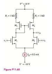
Consider the diff-amp in Figure P11.68. The PMOS parameters are:
(a)
The open circuit differential mode voltage gain.
Answer to Problem 11.68P
The value of the differential mode voltage gain is
Explanation of Solution
Given:
The given circuit is shown in Figure 1
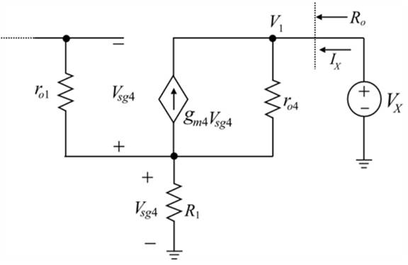
Figure 1
Calculation:
From above, the expression for the source to gate voltage is given by,
Apply KCL at node
Substitute
The expression for the transconductance of the second transistor is evaluated as,
Substitute
The internal output resistance of the second transistor is given by,
Substitute
The expression for the transconductance of the fourth transistor is evaluated as,
Substitute
The internal output resistance of the fourth transistor is given by,
Substitute
The expression to determine the value of the resistance
Substitute
The expression to determine the value of the open circuit differential mode voltage gain is given by,
Substitute
Conclusion:
Therefore, the value of the open circuit differential mode voltage gain is
(b)
To compare: The value of the open circuit differential mode voltage gain for the given changes with the value obtained in part (a).
Answer to Problem 11.68P
The value of the differential voltage gain is
Explanation of Solution
Given:
The given circuit is shown in Figure 1
Figure 1
The value of resistance
Calculation:
When
The expression for the open circuit differential mode voltage gain is given by,
Substitute
When the resistance
Conclusion:
Therefore, the value of the differential voltage gain is
(c)
The value of the output resistance of the differential amplifier for part (a) and (b).
Answer to Problem 11.68P
The differential output resistance of the amplifier for part (a) is
Explanation of Solution
The given circuit is shown in Figure 1

Figure 1
Calculation:
The output resistance for the differential amplifier for the open circuit differential voltage gain is calculated as,
Substitute
The output resistance for the differential amplifier when
Substitute
Conclusion:
Therefore, the differential output resistance of the amplifier is
Want to see more full solutions like this?
Chapter 11 Solutions
Microelectronics: Circuit Analysis and Design


- What change(s), if any, can be introduced into the circuit shown below for a) zero bias? b) depletion- mode bias? c) enhancement- mode bias?arrow_forwardIn the push-pull stage given (in the photo attached), IS1 = 5 × 10⁻¹⁷ A and IS2 = 8 × 10⁻¹⁷ A. Calculate the value of VB so as to establish a bias current of 5 mA in Q1 and Q2 (for Vout = 0). If the peak input swing is 2 V and RL = 8Ω : Calculate the small-signal voltage gain for Vout ≈ 0 Use the gain obtained in (i) to estimate the output voltage swing. Estimate the peak collector current of Q1 assuming that Q2 still carries 5 mAarrow_forwardFor the differential amplifier circuit below, all transistors are identical ( ?≠0 ) a) Draw the single-sided differential mode equivalent circuit, showing all details and labels Explain how you obtained this equivalent circuitarrow_forward
- If RB=12KΩ, RC=150Ω, VBB=7V, VCC=18V determine the IB, IC, IE and collector – emitter voltage in the circuit given below. The transistor has a gain (β) =150. Assume forward voltage drop of the BE junction is 0.7 V (Fig Q2 (d))arrow_forwardThe transistor parameters for the NMOS common source amplifier given in the figure are VTN = 1.0V, kn = 0.8mA / V2 and alpha = 0. Circuit parameters are VDD = 10V, RS = 0.8k, RD = 3K, R1 = 210K and R2 = 140k. Find the IDQ drain current and VDSQ drain-source voltage at the transistor's Q - operating point. Determine in which region the transistor is operating.arrow_forwardInstruction/s: Draw, Illustrate and label your schematic diagram before solving the problem.2.) Given a Collector -Feedback Biased transistor circuit with voltage at common collector is +10v ,base resistor is 100k ohms, Collector resistor is 10k ohms and Base current is 8.38 micro ampere, ,Voltage at Base-emitter junction is 0.7v. Determine Beta DC , Collector current and Voltage at collector-emitter junction. These might help as a guide to answer the problem...arrow_forward
- (a) What are the Q-points for the transistors in the amplifier as shown if VDD = 9 V, VSS = 9 V, ISS = 40 μA, RSS = 1.25 MΩ, and RD = 300 kΩ? Assume Kp = 200 μA/V2, γ = 0.6 V0.5, 2φF = 0.6 V, and VTO = −1 V. (b) What are the differential-mode gain, common-mode gain, CMRR, and differential-mode and common-mode input resistances?arrow_forwardIn the Mosfet circuit given below, R1+R2=50 kΩ, RD= 7.5 kΩ, VDD= 5V, VTP= -0.8 V, Kp= 0.2 mA/V2 is given. Calculate the ID current by determining the working region of the mosfet.arrow_forwardRefer to the differential amplifier circuit shown below . Determine the quiescent DC voltage at the collector terminal of each transistor assuming VBE of two transistor are negligible. What will be the quiescent DC values if VBE is taken to be 0.7 V.arrow_forward
- According to the circuit given below, the values of the parameters specified in the options are detailed. Calculate by solving. (VCC= 12V, Rs = 4.7 K&,R1 = 27 K&,R2 = 5.6K&, RC = 2.2 KQ,RE - 470&, RL=1K&,B= 140) a) What is the current IE? b) What is the re resistance? C) What is the intrinsic gain of the transistor? d) What is the voltage gain of the circuit? e) What is the current gain of the circuit?arrow_forwardConsider the emitter follower in Figure 1 with VCC = 10V, I = 100 mA, and RL = 100Ω. (a) Find the power dissipated in Q1 and Q2 under quiescent conditions. (vO = 0V) (b) For a sinusoidal output voltage of maximum possible amplitude (neglecting VCEsat ), find the average power dissipation in Q1 and Q2. Also find the load power.arrow_forward(a) What are the Q-points for the transistors in the amplifier as shown if VDD = 12V, VSS = 12V, ISS = 1.5 mA, RSS = 33 kΩ, and RD = 15 kΩ? Assume Kn = 375 μA/V2 and VT N = 0.75 V. (b) What are the differential-mode gain, commonmode gain, CMRR, and differential-mode and common-mode input resistances?arrow_forward
 Introductory Circuit Analysis (13th Edition)Electrical EngineeringISBN:9780133923605Author:Robert L. BoylestadPublisher:PEARSON
 Delmar's Standard Textbook Of ElectricityElectrical EngineeringISBN:9781337900348Author:Stephen L. HermanPublisher:Cengage Learning
 Programmable Logic ControllersElectrical EngineeringISBN:9780073373843Author:Frank D. PetruzellaPublisher:McGraw-Hill Education
 Fundamentals of Electric CircuitsElectrical EngineeringISBN:9780078028229Author:Charles K Alexander, Matthew SadikuPublisher:McGraw-Hill Education
 Electric Circuits. (11th Edition)Electrical EngineeringISBN:9780134746968Author:James W. Nilsson, Susan RiedelPublisher:PEARSON
 Engineering ElectromagneticsElectrical EngineeringISBN:9780078028151Author:Hayt, William H. (william Hart), Jr, BUCK, John A.Publisher:Mcgraw-hill Education,