
Videos
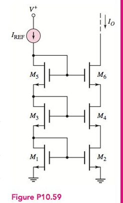
Consider the NMOS current source in Figure P10.59. Let
Want to see the full answer?
Check out a sample textbook solution
Chapter 10 Solutions
Microelectronics: Circuit Analysis and Design


- 9. Design a biased-transistor circuit using VBB = Vcc= 10 V for a Q-point of Ic = 5 mA and VCE 4 V. Assume pc = 100. The design involves finding RB, RC, and the minimum power rating of the transistor. (The actual power rating should be greater.) Sketch the circuit.arrow_forwardVcC R2 RC- RI RL R1 RE VEE Assume: B=100, VA=150, Vcc=12V, VɛE=GND, R=2K, R1=160K, R2=300K, Rɛ=3K, Rc=2.2K, and R1=100K. A.)For the circuit draw the AC equivalent circuit (including the small signal model for the transistor). Then compute r„, ľo, and gm. Then compute Av (the gain for the entire circuit), and Rin (for the whole circuit). B.)Convert the circuit to a common-collector circuit. Draw the new circuit (assume the same values for the input and load resistances). Then compute the terminal voltage gain, and Rin (for the whole circuit), re-computing any parameters that you need to solve.arrow_forward40 The transistor shown in Figure P10.40 has Vy = 0.6 V. Determine values for R1 and R2 such that a. The DC collector-emitter voltage, VceỌ, İs 5 V. b. The DC collector current, Ico, will vary no more than 10% as B varies from 20 to 50. c. Values of R1 and R2 which will permit maximum symmetrical swing in the collector current. Assume B = 100.arrow_forward
- Draw, Illustrate and label your schematic diagram before solving the problem. 3) Given an Emitter-Stabilize Biased transistor circuit with beta DC is 250,Base resistor is 150 ohms, collector resistor is 1.5k ohms ,emitter resistor is 500 ohms ,emitter voltage supply is -5v and Voltage at common collector is +28V,Voltage at Base-emitter junction is 0.7v,. Determine Base current, Collector current and Voltage at collector-emitter junction.arrow_forward1. Calculate the component values necessary to give the design of a Class B common emitter amplifier based on BC109 or equivalent. The nominal voltage gain should be 5 and the input signal should be 0.2 Vpeak-peak. Given such a general specification itarrow_forwardDraw, Illustrate and label your schematic diagram before solving the problem. 1) Given a Fixed-Biased transistor circuit with Beta DC is 200 , voltage at common collector is +22v ,base supply voltage is +11V, Base resistor is 47kOhms , collector resistor is 390 ohms ,Voltage at Base-emitter junction is 0.7v. Determine the Q-point of collector current and Voltage at collector-emitter junction. These might be help as a guide to solve the problem.arrow_forward
- 10 Given the circuit of Figure P10.10, assume both transistors are silicon-based with B = 100. Determine: a. Icı, Vcı, VCEI b. Icz, Vcz, VCrzarrow_forwardWhat are the advantages of active load with respect to passive load in transistors? Write down at least 5 advantages.arrow_forwardConsider a MOSFET circuit with transistor parameters VTN=0.8V, KN=0.85 mA/V and A=0.02V-1. i) Determine Rs and RD such that IDo=0.15mA and VDSQ=5.5V ii) Calculate the small signal parameters i) Draw the small signal equivalent circuit and determine the voltage gain. +5V RD Co O +Vo +Vi RL=50K VGs RG Rs -5V Figure Q4barrow_forward
- Consider the circuit. The transistor has a parameter β that varies between 50 and 200. The operation of the circuit and the electrical variables at the end points must be known. end points. Calculate the following for β = 50 and β = 200. a) lE, VE and VB (DC analysis). b) The input resistance Rin (small signal analysis). c) Voltage gain V0/ Vsig (Small Signal Analysisarrow_forwardIn the figure, A characteristics curve is shown for the MOSFET. Determine the following outcome and parameters using the values given in the characteristics: i) Find the Ip for the VGs = 4V, where IGs(ON) = 4.5mA ii) Find the transconductence of MOSFET; where, MOSFET having the bias voltage VGs = 4V, and 6V. %3D A (mA) A5 (mA) 10 10 VGs=+8 V 9. 7 .7 VGs =+7 V 6 5 Vas=+6 V 4 VGs =+5 V 2 VGs =+4 V Vas =+3 V 1 3 4. 5 8 Vas 10 15 20 25 Vos Vas = VT=2 V a coarrow_forwardWhat are the major differences between the collector characteristics of a BJT transistor and the drain characteristics of a JFET transistor? Describe in your own words why IG is effectively zero amperes for a JFETtransistor. Why is the input impedance to a JFET so high? Why is the terminology field effect appropriate for this important three-terminal device?arrow_forward
 Introductory Circuit Analysis (13th Edition)Electrical EngineeringISBN:9780133923605Author:Robert L. BoylestadPublisher:PEARSON
 Delmar's Standard Textbook Of ElectricityElectrical EngineeringISBN:9781337900348Author:Stephen L. HermanPublisher:Cengage Learning
 Programmable Logic ControllersElectrical EngineeringISBN:9780073373843Author:Frank D. PetruzellaPublisher:McGraw-Hill Education
 Fundamentals of Electric CircuitsElectrical EngineeringISBN:9780078028229Author:Charles K Alexander, Matthew SadikuPublisher:McGraw-Hill Education
 Electric Circuits. (11th Edition)Electrical EngineeringISBN:9780134746968Author:James W. Nilsson, Susan RiedelPublisher:PEARSON
 Engineering ElectromagneticsElectrical EngineeringISBN:9780078028151Author:Hayt, William H. (william Hart), Jr, BUCK, John A.Publisher:Mcgraw-hill Education,