
Videos
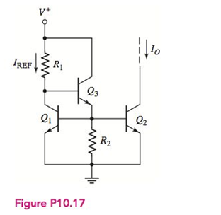
Consider the circuit in Figure P10.17. The transistor parameters are:
Want to see the full answer?
Check out a sample textbook solution
Chapter 10 Solutions
Microelectronics: Circuit Analysis and Design


- Design a circuit to simulate the following mathematical equation using minimum number of operational amplifiers. 5f Vout = 12V1 +5 V2 dt + 6 Where Vout is the output voltage, V1 and V2 are the input voltages. Assume that the available Dc source is +/- 5 volt.arrow_forwardFor the MOSFET circuit given here, V to = 2V, K = 160μA/V2. Design the values of R1 and R2 such that the drain current (ID) is 0.5mAand the current through the R1 and R2 is one-tenth of ID. Assume the transistor isin saturation (Hint: μ = 1 x 10⁻⁶).arrow_forward%3D For the amplifier circuit shown below, let Rg-100 Ko, Vcc=10 V and B=100, then answer the following: RB Cc R. ww V. Vi RE a) Name the configuration of this amplifier b) Find the value of Re so that the DC operating point is in the middle of the load line twwarrow_forward
- 1. Use the figure below to solve following questions (a) Solve the following dc quantitiesi. VB(Q1)ii. VE(Q1)iii. IE(Q1)iv. VC(Q1)v. VB(Q2)vi. VE(Q2)vii. IE(Q2)viii. VC(Q2)(b) Suppose that the emitter follower is omitted and the output from thecollector of Q1 is capacitively coupled to the 250Ω load, RL. What isthe output voltage across the 250Ω load?arrow_forwardConsider the emitter follower in Figure 1 with VCC = 10V, I = 100 mA, and RL = 100Ω. (a) Find the power dissipated in Q1 and Q2 under quiescent conditions. (vO = 0V) (b) For a sinusoidal output voltage of maximum possible amplitude (neglecting VCEsat ), find the average power dissipation in Q1 and Q2. Also find the load power.arrow_forwardThe amplifier circuit shown below has R₁ = 10k, R₂ = 12kN, R₁ = 0.5 kn, Rc = 0.2 kn, and Vcc= 5V. The value of ß = 50 whereas VBE = 0.7V. Determine: a) The Q-point (i.e., IB, IC,IE and VCE). b) Draw the resulting DC load line. Vs HH C₁ R₁ R2 ww ww +Va сс www RC C₂ RL wwwarrow_forward
- 6. A BJT current source is designed as shown below, where QREF= Q₁. If IREF= 5 mA, determine Rp to have I₁= 2 mA (neglect the base current). 4. /REF QREF Vcc + Ка Rparrow_forwardIn the circuit shown , the transistor has a ß of 100, VT = 26mV, and VEB = 0.7V. i) Write the 5 steps required to solve such a problem. ii) Find Rin iii) Use T Model to Find the overall voltage gain (vo/Vsig) iv) For an output signal of +0.4 V, what values of vsig i and vp are required? +5 V +1.5 V ) 10 mA 10 kN Rig 1 kN Vsig Rc 100 Narrow_forwardA simple circuit using an NMOS transistor is snown in the on as an amplifier. The input signal is vs, and the output signal is ip (mA) 40 RDmaz = 30 20 the output voltage for a given input voltage. The load line is a | Kirchhoff's voltage law around the drain loop. By plotting this line he intersection of the two graphs. An example of the resulting graph 10 Load line Part B - Choose the drain resistor ΠΠ ΑΣΦ 333.3 5 Submit Previous Answers Hilt ↓↑ vec 3 V GG X Incorrect; Try Again; 5 attempts remaining 10 RD W Ω Holt 15 The gate bias voltage is chosen to be VGG = 4 V and the drain bias voltage is chosen to be VDD = 20 V. What is the largest value that can be used for RD to keep the transistor in the saturation region? Express your answer to three significant figures. ▸ View Available Hint(s) VDD UGS = 5.5 20 UDS (V)arrow_forward
- Electrical Engineering Please solve ASAP 1. The figure shows a CE power amplifier in which the collector resistor serves also as the load resistor. Assume Boc = Be = 120. +12 V a) Determine the de Q-point (Icq and Vcr). Re 470 1 b) Determine the voltage gain and the power gain. R 12 kn c) The Quiescent power. 10 uF d) The i'p signal power 10 F RE 220 e) The output signal power. 400 mV pp 1.0 kHz ) The efficiency of the power amplifier. R2 4.7 k Ru 120 2 10 uF 470 1 Ba- Boc= 120arrow_forwardV* = + |ov Ri Rip ERC Vs RE V: -sV The following parameters are given for this transistor: B = 200 and VA = o. Design the circuit with the following value ICQ = 1.5mA and VCEQ = 5V. Find the small signal voltage gain AV = Vo/Vs. Find the input resistance in the signal source Vs.arrow_forward5V B OV OV For all the MOSFETS assume Vth=1V and k =50 mA/V² R₁ = 4700 Ao M₁ M₂ B Indicate and verify the state of each MOSFET and Vo for the following input combinations. Fill out the table for each assumed state of the MOSFET for every input combination. Use Rds(on) approximation for linear operation and three significant figures for the voltages. M1 is assumed to be in saturation. If Vgs = 2 V, Vds = 4V, Vds > Vgs - Vth 4>2-1 4> 1 (ok) Vgs > Vth (2>1) A M2 state M3 state V. 0 OV 5 V R₂ = 560Ω 5V M1 state M3arrow_forward
 Introductory Circuit Analysis (13th Edition)Electrical EngineeringISBN:9780133923605Author:Robert L. BoylestadPublisher:PEARSON
 Delmar's Standard Textbook Of ElectricityElectrical EngineeringISBN:9781337900348Author:Stephen L. HermanPublisher:Cengage Learning
 Programmable Logic ControllersElectrical EngineeringISBN:9780073373843Author:Frank D. PetruzellaPublisher:McGraw-Hill Education
 Fundamentals of Electric CircuitsElectrical EngineeringISBN:9780078028229Author:Charles K Alexander, Matthew SadikuPublisher:McGraw-Hill Education
 Electric Circuits. (11th Edition)Electrical EngineeringISBN:9780134746968Author:James W. Nilsson, Susan RiedelPublisher:PEARSON
 Engineering ElectromagneticsElectrical EngineeringISBN:9780078028151Author:Hayt, William H. (william Hart), Jr, BUCK, John A.Publisher:Mcgraw-hill Education,