
Microelectronics: Circuit Analysis and Design
4th Edition
ISBN: 9780073380643
Author: Donald A. Neamen
Publisher: McGraw-Hill Companies, The
expand_more
expand_more
format_list_bulleted
Videos
Textbook Question
Chapter 10, Problem 10.16P
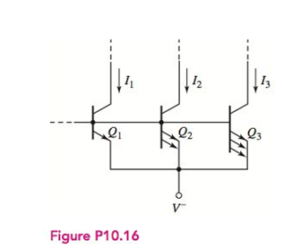
The values of  for the transistors in Figure P10.16 are very large. (a) if
  is diode-connected with
  determine the collector currents inthe other two transistors. (b) Repeat part (a) if
  is diode-connected with
 (e) Repeat part (a) if
  is diode-connected with
Expert Solution & Answer
Want to see the full answer?
Check out a sample textbook solution
Students have asked these similar questions
- Explain the effect of base resistance and collector resistance on the circuit.
How collector current in BJT depend on different parameter.
Describe how collector current change due o chnage in Ico.
What are the advantages of active load with respect to passive load in
transistors? Write down at least 5 advantages.
Chapter 10 Solutions
Microelectronics: Circuit Analysis and Design
Ch. 10 - The circuit parameters for the two-transistor...Ch. 10 - Consider the circuit shown in Figure 10.3. The...Ch. 10 - The parameters of the circuit shown in Figure 10.5...Ch. 10 - Consider the Widlar current source in Figure 10.9....Ch. 10 - Consider the circuit in Figure 10.10. Assume the...Ch. 10 - A Widlar current source is shown in Figure 10.9....Ch. 10 - Figure 10.12 shows the N-output current mirror....Ch. 10 - Prob. 10.1TYUCh. 10 - Prob. 10.2TYUCh. 10 - For the Wilson current source in Figure 10.8, the...
Ch. 10 - Prob. 10.4TYUCh. 10 - Prob. 10.8EPCh. 10 - Prob. 10.9EPCh. 10 - Consider the JFET circuit in Figure 10.24. The...Ch. 10 - Consider Design Example 10.8. Assume transistor...Ch. 10 - The bias voltages of the MOSFET current source in...Ch. 10 - Prob. 10.7TYUCh. 10 - All transistors in the MOSFET modified Wilson...Ch. 10 - A simple BJT amplifier with active load is shown...Ch. 10 - Prob. 10.9TYUCh. 10 - Prob. 10.10TYUCh. 10 - Prob. 10.11TYUCh. 10 - Prob. 10.12EPCh. 10 - For the circuit in Figure 10.40(a), the transistor...Ch. 10 - Prob. 10.12TYUCh. 10 - Repeat Example 10.12 for the case where a resistor...Ch. 10 - Prob. 10.14TYUCh. 10 - Prob. 1RQCh. 10 - Explain the significance of the output resistance...Ch. 10 - Prob. 3RQCh. 10 - Prob. 4RQCh. 10 - What is the primary advantage of a BJT cascode...Ch. 10 - Prob. 6RQCh. 10 - Can a piecewise linear model of the transistor be...Ch. 10 - Prob. 8RQCh. 10 - Sketch the basic MOSFET two-transistor current...Ch. 10 - Discuss the effect of mismatched transistors on...Ch. 10 - Prob. 11RQCh. 10 - Sketch a MOSFET cascode current source circuit and...Ch. 10 - Discuss the operation of an active load.Ch. 10 - What is the primary advantage of using an active...Ch. 10 - Prob. 15RQCh. 10 - What is the impedance seen looking into a simple...Ch. 10 - What is the advantage of using a cascode active...Ch. 10 - Prob. 10.1PCh. 10 - The matched transistors Q1 and Q2 in Figure...Ch. 10 - Prob. 10.3PCh. 10 - Reconsider the circuit in Figure 10.2(a). Let...Ch. 10 - Prob. 10.5PCh. 10 - The transistor and circuit parameters for the...Ch. 10 - The bias voltages in the circuit shown in Figure...Ch. 10 - Consider the current source in Figure 10.2(b). The...Ch. 10 - Prob. 10.9PCh. 10 - Prob. 10.10PCh. 10 - Prob. D10.11PCh. 10 - In the circuit in Figure P10.11, the transistor...Ch. 10 - Prob. D10.13PCh. 10 - Consider the circuit shown in Figure P 10.14. The...Ch. 10 - Design a basic two-transistor current...Ch. 10 - The values of for the transistors in Figure P10.16...Ch. 10 - Consider the circuit in Figure P10.17. The...Ch. 10 - All transistors in the N output current mirror in...Ch. 10 - Design a pnp version of the basic three-transistor...Ch. 10 - Prob. D10.20PCh. 10 - Consider the Wilson current source in Figure...Ch. 10 - Consider the circuit in Figure P10.22. The...Ch. 10 - Consider the Wilson current-source circuit shown...Ch. 10 - Consider the Widlar current source shown in Figure...Ch. 10 - Prob. 10.25PCh. 10 - Consider the circuit in Figure P10.26. Neglect...Ch. 10 - (a) For the Widlar current source shown in Figure...Ch. 10 - Consider the Widlar current source in Problem...Ch. 10 - (a) Design the Widlar current source such that...Ch. 10 - Design a Widlar current source to provide a bias...Ch. 10 - Design the Widlar current source shown in Figure...Ch. 10 - The circuit parameters of the Widlar current...Ch. 10 - Consider the Widlar current source in Figure 10.9....Ch. 10 - Consider the circuit in Figure P10.34. The...Ch. 10 - The modified Widlar current-source circuit shown...Ch. 10 - Consider the circuit in Figure P10.36. Neglect...Ch. 10 - Consider the Widlar current-source circuit with...Ch. 10 - Assume that all transistors in the circuit in...Ch. 10 - In the circuit in Figure P10.39, the transistor...Ch. 10 - Consider the circuit in Figure P10.39, with...Ch. 10 - Consider the circuit shown in Figure P10.41....Ch. 10 - For the circuit shown in Figure P 10.42, assume...Ch. 10 - Consider the circuit in Figure P10.43. The...Ch. 10 - Consider the MOSFET current-source circuit in...Ch. 10 - The MOSFET current-source circuit in Figure P10.44...Ch. 10 - Consider the basic two-transistor NMOS current...Ch. 10 - Prob. 10.47PCh. 10 - Consider the circuit shown in Figure P10.48. Let...Ch. 10 - Prob. 10.49PCh. 10 - The circuit parameters for the circuit shown in...Ch. 10 - Prob. 10.51PCh. 10 - Figure P10.52 is a PMOS version of the...Ch. 10 - The circuit shown in Figure P10.52 is biased at...Ch. 10 - The transistor circuit shown in Figure P10.54 is...Ch. 10 - Assume the circuit shown in Figure P10.54 is...Ch. 10 - The circuit in Figure P 10.56 is a PMOS version of...Ch. 10 - The transistors in Figure P10.56 have the same...Ch. 10 - Consider the NMOS cascode current source in Figure...Ch. 10 - Consider the NMOS current source in Figure P10.59....Ch. 10 - Prob. 10.60PCh. 10 - The transistors in the circuit shown in Figure...Ch. 10 - A Wilson current mirror is shown in Figure...Ch. 10 - Repeat Problem 10.62 for the modified Wilson...Ch. 10 - Prob. 10.64PCh. 10 - Prob. 10.65PCh. 10 - Prob. D10.66PCh. 10 - Prob. D10.67PCh. 10 - The parameters of the transistors in the circuit...Ch. 10 - Prob. 10.69PCh. 10 - Consider the circuit shown in Figure P10.70. The...Ch. 10 - Prob. 10.71PCh. 10 - Prob. D10.72PCh. 10 - Prob. 10.73PCh. 10 - Prob. D10.74PCh. 10 - Prob. 10.75PCh. 10 - For the circuit shown in Figure P10.76, the...Ch. 10 - Prob. 10.77PCh. 10 - Prob. 10.78PCh. 10 - The bias voltage of the MOSFET amplifier with...Ch. 10 - Prob. 10.80PCh. 10 - Prob. 10.81PCh. 10 - Prob. 10.82PCh. 10 - A BJT amplifier with active load is shown in...Ch. 10 - Prob. 10.84PCh. 10 - Prob. 10.85PCh. 10 - Prob. 10.86PCh. 10 - The parameters of the transistors in Figure P10.87...Ch. 10 - The parameters of the transistors in Figure P10.88...Ch. 10 - A BJT cascode amplifier with a cascode active load...Ch. 10 - Design a bipolar cascode amplifier with a cascode...Ch. 10 - Design a MOSFET cascode amplifier with a cascode...Ch. 10 - Design a generalized Widlar current source (Figure...Ch. 10 - The current source to be designed has the general...Ch. 10 - Designa PMOS version of the current source circuit...Ch. 10 - Consider Exercise TYU 10.10. Redesign the circuit...
Knowledge Booster


Learn more about
Need a deep-dive on the concept behind this application? Look no further. Learn more about this topic, electrical-engineering and related others by exploring similar questions and additional content below.Similar questions
- For the fixed-bias configuration, determine: a. Base Current b. Collector Current c. Collector-Emitter Voltage d. Collector Voltage e. Base Voltage f. Emitter Voltagearrow_forwardDraw, Illustrate and label your schematic diagram before solving the problem. 3) Given an Emitter-Stabilize Biased transistor circuit with beta DC is 250,Base resistor is 150 ohms, collector resistor is 1.5k ohms ,emitter resistor is 500 ohms ,emitter voltage supply is -5v and Voltage at common collector is +28V,Voltage at Base-emitter junction is 0.7v,. Determine Base current, Collector current and Voltage at collector-emitter junction.arrow_forwardDraw the large-signal dc circuit model for a silicon npn transistor in the active region at room temperature. Include the constraints of currents and voltages that guarantee operation in the active region. Repeat for the saturation region. Repeat for the cutoff region.arrow_forward
- Sketch the general current- voltage characteristics for both enhancement-mode and depletion-mode MOSFETs. Define the saturation and nonsaturation bias regionsarrow_forward1. What is Current Mirror circuit ? Why is it so called? Draw a three MOSFET two stage current mirror and explain how the reference current equals the drain current of the second stage MOSFET.arrow_forwardA Bipolar junction Transistor with curreat amplification factor being 100, Input Base current is 50μA. Collector voltage is 10 V and biasing voltage being +20 V. Find followings a. Collector current b. Resistance (R1) c. Collector voltage , Emitter voltage , Base Voltage & Collector-Emitter Voltage.arrow_forward
- Discuss High level modulator: circuit diagram and operation - Collector modulatorarrow_forwardDescribe the application and use of Junction Field-Effect Transistors (JFETs)arrow_forward9. Design a biased-transistor circuit using VBB = Vcc= 10 V for a Q-point of Ic = 5 mA and VCE 4 V. Assume pc = 100. The design involves finding RB, RC, and the minimum power rating of the transistor. (The actual power rating should be greater.) Sketch the circuit.arrow_forward
- do details steps when for the cutoff and saturation point..arrow_forwardThe small-signal model is said to be valid for voltage variations of about 5 mV. To what percentage current change does this correspond? (Consider both positive and negative signals.) What is the maximum allowable voltage signal (positive or negative) if the current change is to be limited to 10%?arrow_forwardQUESTION 4 For an n-channel Junction Field-Effect Transistor (JFET), the gate-source cut-off voltage, VGS(OFF), is -4 V and the drain saturation current, Ipss is 50 mA. The drain current ID, is 12 mA. Determine the gate-to-source voltage, Vos, of the JFET.arrow_forward
arrow_back_ios
SEE MORE QUESTIONS
arrow_forward_ios
Recommended textbooks for you
 Introductory Circuit Analysis (13th Edition)Electrical EngineeringISBN:9780133923605Author:Robert L. BoylestadPublisher:PEARSON
 Delmar's Standard Textbook Of ElectricityElectrical EngineeringISBN:9781337900348Author:Stephen L. HermanPublisher:Cengage Learning
 Programmable Logic ControllersElectrical EngineeringISBN:9780073373843Author:Frank D. PetruzellaPublisher:McGraw-Hill Education
 Fundamentals of Electric CircuitsElectrical EngineeringISBN:9780078028229Author:Charles K Alexander, Matthew SadikuPublisher:McGraw-Hill Education
 Electric Circuits. (11th Edition)Electrical EngineeringISBN:9780134746968Author:James W. Nilsson, Susan RiedelPublisher:PEARSON
 Engineering ElectromagneticsElectrical EngineeringISBN:9780078028151Author:Hayt, William H. (william Hart), Jr, BUCK, John A.Publisher:Mcgraw-hill Education,
Introductory Circuit Analysis (13th Edition)
Electrical Engineering
ISBN:9780133923605
Author:Robert L. Boylestad
Publisher:PEARSON
Delmar's Standard Textbook Of Electricity
Electrical Engineering
ISBN:9781337900348
Author:Stephen L. Herman
Publisher:Cengage Learning
Programmable Logic Controllers
Electrical Engineering
ISBN:9780073373843
Author:Frank D. Petruzella
Publisher:McGraw-Hill Education
Fundamentals of Electric Circuits
Electrical Engineering
ISBN:9780078028229
Author:Charles K Alexander, Matthew Sadiku
Publisher:McGraw-Hill Education
Electric Circuits. (11th Edition)
Electrical Engineering
ISBN:9780134746968
Author:James W. Nilsson, Susan Riedel
Publisher:PEARSON
Engineering Electromagnetics
Electrical Engineering
ISBN:9780078028151
Author:Hayt, William H. (william Hart), Jr, BUCK, John A.
Publisher:Mcgraw-hill Education,
Diode Logic Gates - OR, NOR, AND, & NAND; Author: The Organic Chemistry Tutor;https://www.youtube.com/watch?v=9lqwSaIDm2g;License: Standard Youtube License