
Videos
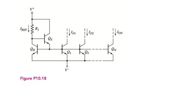
All transistors in the N output current mirror in Figure P10.18 are matched,with a finite
Want to see the full answer?
Check out a sample textbook solution
Chapter 10 Solutions
Microelectronics: Circuit Analysis and Design


- 2 a) i) Draw typical output characteristics of a common emitter npn transistor and clearly identify the active, saturation, and cut off regions on your drawing. ii) Explain how you can find the common emitter de current gain, B, and the common emitter ac current gain, hre, from the common emitter output characteristics of an npn transistor. You need to draw typical output characteristics in scales and provide numerical calculations to support your explanation.arrow_forwardExplain how you can find the common emitter de current gain, B, and the common emitter ac current gain, hre, from the common emitter output characteristics of an npn transistor. You need to draw typical output characteristics in scales and provide numerical calculations to support your explanation.arrow_forwardQ.4/ Refer to the class AB power amplifier shown below:a. Determine the dc parameters VB(Q1), VB(Q2), ICQ, VCEQ(Q1), VCEQ(Q2).b. For the 5Vrms input, determine the power delivered to the load resistor.c. Determine the approximate input resistance seen by the signal source if ac=100arrow_forward
- Q.1/ Figure below shows a CE power amplifier in which the collector resistor serves also as the load resistor. Assume Boc-Bac-100. a. Determines the de Q-point (Ico and VCEO). b. Determine the voltage gain and the power gain. c. What changes would be necessary to convert the circuit to a pnp transistor with a positive supply? What advantage would this have? +Vce +15 V R 100 LO K 0.5 W 22 juF RE 8.2 S00 mV pp 330 1 R 36 0 100 uFarrow_forwardConsider class-A emitter follower circuit shown in the figure below. The circuit parameters are V+ = 24 V, V- = -24 V, and RL = 2000. The transistor parameters are B = 50, VBE(on) = 0.7 V, and VcE(sat) = 0.2 V. The output voltage is to vary between +20 V and -20 V. The minimum current in Q1 is to be iej = 20 mA. For vo = 0, find the dissipated in the first transistor Qr. power RL wwliarrow_forwardConsider the source follower circuit in Figure shown below, IQ = 10 mA VTP = -2 V, Kp = 5mA/V2, RL = 680 n, and 2 = 0.01 V-1. Where Kp=1/2 k'p(W/L). (IV) What is the formula for Vi? (v) Determine the small-signal voltage gain (V/V:). (vi) Find the output resistance Ro. V* = 5 V KL RG= 200 k2 V=-5 V wwarrow_forward
- Open with v Consider class-A emitter follower circuit shown in the figure below. The circuit parameters are V+ = 24 V, V- = -24 V, and RL = 2000. The transistor parameters are B = 50, VBElon) = 0.7 V, and VCElsat) = 0.2 V. The output voltage is to vary between +20 V and -20 V. The minimum current in Q1 is to be ie1 = 20 mA. For vo = 0, find the power dissipated in the first transistor Q1- V+arrow_forwardQ1. (a) Consider the amplifier circuit in Figure Q1(a). Given the following: RI = 100 k2 R2 = 56 kN Rc =2 k2 Vcc = +8 V Assume the transistor has B = 100 and VBE(on) = 0.7 V. You may neglect Early effect and use VT = 26 mV. (i) Draw the DC equivalent circuit, then determine Iç and VCE. Draw the AC equivalent circuit using re model. Based on this, determine the parameters Av, Rin and Rout. (ii) Vcc Rc R1 R2 C3 Vout C2 Ci Vin Figure Q1(a)arrow_forwardIn the circuit shown in the figure, the internal resistance of a voltage source is given as 3 ohms. Load values are such that R = 20 ohms and X = 20 ohms. The effective value of the VAB voltage at the load ends is 220 V. (Frequency is 50 Hz). What is the active power consumed by the load? (Do not take into account 3 ohms in calculations)arrow_forward
- Figure 1 2. For the class B output stage of Figure 2, let Vcc = 6 V and R, = 4N. If the output is a sinusoidal with 4.5V peak amplitude, find; (a) The output power. (b) The average power drawn from each supply/ (c) The power efficiency obtained at this output voltage. (d) The maximum power that each transistor must be capable of dissipating safely. +Vcc RL --Vcc Figure 2arrow_forwardThe amplifier in the circuit below is driven by a signal generator v, with a small sine wave signal vhose average value is zero. Assume the transistor has a value of B-100, and V-26 mV. a. You need to design the circuit so that the de emitter current IE of the emitter resistor RE to establish the desired de emitter current. = 1 mA. Specify the value b. A de collector voltage of +5 volts is desired. Specify the value of the collector resistor Re to establish the desired de collector voltage. For this part assume that RL 5 K and the Early Effect needs to be considered. The transistor has a VA 100 Volts. Draw the ac small signal equivalent circuit model of the amplifier and determine its voltage gain. 91SV C. 2.5k MM do RE -15 V 84 Vout RLarrow_forwardConsider the circuit. The transistor has a parameter β that varies between 50 and 200. The operation of the circuit and the electrical variables at the end points must be known. end points. Calculate the following for β = 50 and β = 200. a) lE, VE and VB (DC analysis). b) The input resistance Rin (small signal analysis). c) Voltage gain V0/ Vsig (Small Signal Analysisarrow_forward
 Introductory Circuit Analysis (13th Edition)Electrical EngineeringISBN:9780133923605Author:Robert L. BoylestadPublisher:PEARSON
 Delmar's Standard Textbook Of ElectricityElectrical EngineeringISBN:9781337900348Author:Stephen L. HermanPublisher:Cengage Learning
 Programmable Logic ControllersElectrical EngineeringISBN:9780073373843Author:Frank D. PetruzellaPublisher:McGraw-Hill Education
 Fundamentals of Electric CircuitsElectrical EngineeringISBN:9780078028229Author:Charles K Alexander, Matthew SadikuPublisher:McGraw-Hill Education
 Electric Circuits. (11th Edition)Electrical EngineeringISBN:9780134746968Author:James W. Nilsson, Susan RiedelPublisher:PEARSON
 Engineering ElectromagneticsElectrical EngineeringISBN:9780078028151Author:Hayt, William H. (william Hart), Jr, BUCK, John A.Publisher:Mcgraw-hill Education,