
Concept explainers
Videos
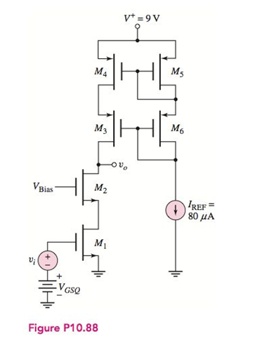
The parameters of the transistors in Figure P10.88 are
Want to see the full answer?
Check out a sample textbook solution
Chapter 10 Solutions
Microelectronics: Circuit Analysis and Design


- 2. This is a small signal problem. Suppose the MOSFETS drawn have lp = 1 mA when VGS = 2.5 V, and Vth = 0.5 V. Suppose the BJTs drawn have Ic = 1 mA when VBE = 0.7 V. Av VDD = 5V VDD VDD T T Rc = 1 kn Vin RB2 = 10 kn RB1 = 10 kn w/li w Rp = 1 kn R₁ Vout (a) Derive voltage gain Ay and input impedance Zin assuming R₁ ➡8. (b) Plot Ay as a function of R, assuming R, is attached between Vout and ground. (c) Rederive Ay and Zin assuming Roo and after swapping the BJT and MOSFET. RLarrow_forwardFrom the figure shown, when S1 is at 1 : up position; the following statement is not correct except: (a) Collector-emitter voltage of Q1 is approximately zero (b) the LED will illuminate (c) the base voltage of Q2 is equal to 9 V (d) (b) and (c)arrow_forward5V B OV OV For all the MOSFETS assume Vth=1V and k =50 mA/V² R₁ = 4700 Ao M₁ M₂ B Indicate and verify the state of each MOSFET and Vo for the following input combinations. Fill out the table for each assumed state of the MOSFET for every input combination. Use Rds(on) approximation for linear operation and three significant figures for the voltages. M1 is assumed to be in saturation. If Vgs = 2 V, Vds = 4V, Vds > Vgs - Vth 4>2-1 4> 1 (ok) Vgs > Vth (2>1) A M2 state M3 state V. 0 OV 5 V R₂ = 560Ω 5V M1 state M3arrow_forward
- Q1. The output characteristic of a typical transistor is shown below, where the quiescent point is selected on it. This transistor is used in the bias circuit presented below. Find the suitable values of Rg and Rc to fix the Q-point of the circuit properly. +Vcc = 12 V 12- Is = 70 uA 10- Ig = 60 uA 8- Rc Is = 50 uA Rs 6- Ig= 40 uA 4. Is = 30 uĄ Is = 20 uA B = 100 2- VBE = 0.7 V 0- -2- 2 4 6 8 10 12 14 16 VCE (V) Ic (mA)arrow_forwardIn the figure, A characteristics curve is shown for the MOSFET. Determine the following outcome and parameters using the values given in the characteristics: i) Find the Ip for the VGs = 4V, where IGs(ON) = 4.5mA ii) Find the transconductence of MOSFET; where, MOSFET having the bias voltage VGs = 4V, and 6V. %3D A (mA) A5 (mA) 10 10 VGs=+8 V 9. 7 .7 VGs =+7 V 6 5 Vas=+6 V 4 VGs =+5 V 2 VGs =+4 V Vas =+3 V 1 3 4. 5 8 Vas 10 15 20 25 Vos Vas = VT=2 V a coarrow_forwardFor the circuit of Figure 2. Carry out the analysis in DC and small signal with www.w www www.www Vt=0.7 V, Kn(W/L) = 4 mA/V. Ignore the Early effect. Determine: (a) The current in DC ID. (b) The gains vo/v₁, io/ii (c) The input resistance Rin and output resistance Rout. wwwwww 06402 www Ca HH {ama Ο ΜΩ www.11 Figura 2: 0.51 k www.li 12 V • 27 ΚΩ Ca +1₁ -0% 4.7 karrow_forward
- Determine the input resistance Rin as indicated in the figure. Ignore resistor ro of the transistor and capacitors are large. A. Rin = R1//R2//R3 B. Rin = R2//R3 (//R4//R5) C. Rin = R2//R3 // ( r π + [1+gm r π ] (//R4//R5) ) D. Rin = R2//R3 // r π (//R4//R5) )arrow_forwardDraw, Illustrate and label your schematic diagram before solving the problem. 3) Given an Emitter-Stabilize Biased transistor circuit with beta DC is 250,Base resistor is 150 ohms, collector resistor is 1.5k ohms ,emitter resistor is 500 ohms ,emitter voltage supply is -5v and Voltage at common collector is +28V,Voltage at Base-emitter junction is 0.7v,. Determine Base current, Collector current and Voltage at collector-emitter junction.arrow_forwardIn reference to the given figure, VCB = 10.3V and VBE = 0.7V. NOTES: VCB = VC-VB VBE = VB-VE In reference to Figure 2, given the dc load line and the transistor circuit, what will be the value of RC, in kilo-ohms? In reference to Figure 2, given the dc load line and the transistor circuit, what will be the voltage of RB, in volts? In reference to Figure 2, given the dc load line and the transistor circuit, what will be the value of RB in kilo-ohms, if Beta=100?arrow_forward
- Using LTSpice, simulate the circuit below, use 2N3904 for the transistor. Part ! DC simulation: Measure VCE and Ic. Use .op for the simulation cmd. Remove all capacitors and input signals first. Part 2 AC simulation: Connect all capacitors now and apply an AC signal at the input with an amplitufe of 1mV and a frequency of 1kHz. Determine the Voltage gain of the circuit by dividing Vo with Vin. Show the output for both the DC and AC analysis. Take a screenshot of the circuit and the output voltages and waveforms. Paste in a word file, write your answers, then save as pdf. 50 kΩ Σ 20 0,5 ΚΩ wwwh 9 Vcc=20 V Ca=1 µF = Cc₂ Cg=50 μF 5.6 kn B=100 Ca IST • 3.3 ΚΩ 5 ΚΩΣ CEarrow_forwardDesign counter 0,2,4,6,… with JKFF and DFFarrow_forwardA certain npn silicon transistor has vBE=0.7 V for iB=0.1 mA at a temperature of 30°C. Sketch the input characteristic to scale at 30°C. What is the approximate value of vBE for iB = 0.1 mA at 180°C? (Use the rule of thumb that vBE is reduced in magnitude by 2 mV per degree increase in temperature.) Sketch the input characteristic to scale at 180°C.arrow_forward
 Introductory Circuit Analysis (13th Edition)Electrical EngineeringISBN:9780133923605Author:Robert L. BoylestadPublisher:PEARSON
 Delmar's Standard Textbook Of ElectricityElectrical EngineeringISBN:9781337900348Author:Stephen L. HermanPublisher:Cengage Learning
 Programmable Logic ControllersElectrical EngineeringISBN:9780073373843Author:Frank D. PetruzellaPublisher:McGraw-Hill Education
 Fundamentals of Electric CircuitsElectrical EngineeringISBN:9780078028229Author:Charles K Alexander, Matthew SadikuPublisher:McGraw-Hill Education
 Electric Circuits. (11th Edition)Electrical EngineeringISBN:9780134746968Author:James W. Nilsson, Susan RiedelPublisher:PEARSON
 Engineering ElectromagneticsElectrical EngineeringISBN:9780078028151Author:Hayt, William H. (william Hart), Jr, BUCK, John A.Publisher:Mcgraw-hill Education,