
Concept explainers
Videos
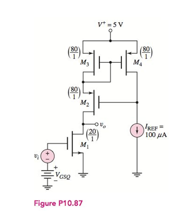
The parameters of the transistors in Figure P10.87 are
Want to see the full answer?
Check out a sample textbook solution
Chapter 10 Solutions
Microelectronics: Circuit Analysis and Design


- For the circult shown in the given figure. Rc-2.4 k0, Rg-10 ko. Pmin-50, and Vcc=5 V. Determine the range of values of Vgg 50 Ic that the transistor is in saturation. Assume Vy-0.6 V and VCEsat -0.2 V. The range of values of VB8 Is VBB> 12 V Ra VAR со Va VCE OE RC Nccarrow_forwardQ1. The output characteristic of a typical transistor is shown below, where the quiescent point is selected on it. This transistor is used in the bias circuit presented below. Find the suitable values of Rg and Rc to fix the Q-point of the circuit properly. +Vcc = 12 V 12- Is = 70 uA 10- Ig = 60 uA 8- Rc Is = 50 uA Rs 6- Ig= 40 uA 4. Is = 30 uĄ Is = 20 uA B = 100 2- VBE = 0.7 V 0- -2- 2 4 6 8 10 12 14 16 VCE (V) Ic (mA)arrow_forwardDetermine the input resistance Rin as indicated in the figure. Ignore resistor ro of the transistor and capacitors are large. A. Rin = R1//R2//R3 B. Rin = R2//R3 (//R4//R5) C. Rin = R2//R3 // ( r π + [1+gm r π ] (//R4//R5) ) D. Rin = R2//R3 // r π (//R4//R5) )arrow_forward
- At any point on the characteristics the product of VCE and IC must be equal to 300 mW. If we choose IC to be the maximum value of 50 mA and substitute into the relationship above, we obtain VCE=? VCEIC = 300 mW a. Reverse bias (J1) and Forward bias (J2) b. Forward bias (J1) and Reverse bias (J2) c.Reverse bias (J1) and Reverse bias (J2) d. Forward bias (J1) and Forward bias (J2)arrow_forwardShow the Common Emitter amplified output when sinusoidal 100Hz signal is applied at the input capacitor. Plz show the circuit diagramarrow_forwardFor the circuit shown below, sketch the DC and AC load lines and determine the operating point (Q-point). Vcc +12V R, Rc CH1 10K 2.7K Cout Vout CH2 Cin BC107 2.2µF Vs 2.2µF RE1 R 0.2Vp R2 1202 10K 3.3K f= 10KHZ RE2 CE 1K 10µFarrow_forward
- Using the re model circuit, determine the total voltage gain for the BJT circuit shown below. Show the details of your work. 22V ... 5.6k0 330k Vo + 10UF-POL B = 80 1200 10UF-POL To = 40 kN 2N2221 6.8k) Vs 4700 22UF-POLarrow_forwardFor the circuit of Figure 2. Carry out the analysis in DC and small signal with www.w www www.www Vt=0.7 V, Kn(W/L) = 4 mA/V. Ignore the Early effect. Determine: (a) The current in DC ID. (b) The gains vo/v₁, io/ii (c) The input resistance Rin and output resistance Rout. wwwwww 06402 www Ca HH {ama Ο ΜΩ www.11 Figura 2: 0.51 k www.li 12 V • 27 ΚΩ Ca +1₁ -0% 4.7 karrow_forwardQ1. For the MOSFET circuit below, input is sinusoidal signal of amplitude IV and frequency 50Hz. Find, the DC operating point, Plot the frequency response and Plot the input, output and transfer characteristics and find out the small signal equivalent. Assume an overdrive voltage of 0.2V Use MOSFET 500nm Library file provided. F Vdd=5V -=80 K R1 (1 1.20Farrow_forward
- Determine Vx and the mode of operation of the PNP transistor shown in the figure below. Assume Is = °A, B = 50, VA = 00, and Rc = 0.1 KO. 10x10-16 %3D Vcc는 2 V 1.2 V- Rc Select one: a. 0.577 V, Active Mode O b. 0.23 V, Active Mode O c. None of these d. 1.153 V, Active Mode e. 2.306 V, Saturation Modearrow_forwardA simple circuit using an NMOS transistor is snown in the on as an amplifier. The input signal is vs, and the output signal is ip (mA) 40 RDmaz = 30 20 the output voltage for a given input voltage. The load line is a | Kirchhoff's voltage law around the drain loop. By plotting this line he intersection of the two graphs. An example of the resulting graph 10 Load line Part B - Choose the drain resistor ΠΠ ΑΣΦ 333.3 5 Submit Previous Answers Hilt ↓↑ vec 3 V GG X Incorrect; Try Again; 5 attempts remaining 10 RD W Ω Holt 15 The gate bias voltage is chosen to be VGG = 4 V and the drain bias voltage is chosen to be VDD = 20 V. What is the largest value that can be used for RD to keep the transistor in the saturation region? Express your answer to three significant figures. ▸ View Available Hint(s) VDD UGS = 5.5 20 UDS (V)arrow_forwardUsing LTSpice, simulate the circuit below, use 2N3904 for the transistor. Part ! DC simulation: Measure VCE and Ic. Use .op for the simulation cmd. Remove all capacitors and input signals first. Part 2 AC simulation: Connect all capacitors now and apply an AC signal at the input with an amplitufe of 1mV and a frequency of 1kHz. Determine the Voltage gain of the circuit by dividing Vo with Vin. Show the output for both the DC and AC analysis. Take a screenshot of the circuit and the output voltages and waveforms. Paste in a word file, write your answers, then save as pdf. 50 kΩ Σ 20 0,5 ΚΩ wwwh 9 Vcc=20 V Ca=1 µF = Cc₂ Cg=50 μF 5.6 kn B=100 Ca IST • 3.3 ΚΩ 5 ΚΩΣ CEarrow_forward
 Introductory Circuit Analysis (13th Edition)Electrical EngineeringISBN:9780133923605Author:Robert L. BoylestadPublisher:PEARSON
 Delmar's Standard Textbook Of ElectricityElectrical EngineeringISBN:9781337900348Author:Stephen L. HermanPublisher:Cengage Learning
 Programmable Logic ControllersElectrical EngineeringISBN:9780073373843Author:Frank D. PetruzellaPublisher:McGraw-Hill Education
 Fundamentals of Electric CircuitsElectrical EngineeringISBN:9780078028229Author:Charles K Alexander, Matthew SadikuPublisher:McGraw-Hill Education
 Electric Circuits. (11th Edition)Electrical EngineeringISBN:9780134746968Author:James W. Nilsson, Susan RiedelPublisher:PEARSON
 Engineering ElectromagneticsElectrical EngineeringISBN:9780078028151Author:Hayt, William H. (william Hart), Jr, BUCK, John A.Publisher:Mcgraw-hill Education,