
Videos
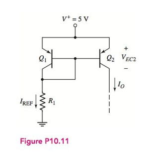
In the circuit in Figure P10.11, the transistor parameters are
Want to see the full answer?
Check out a sample textbook solution
Chapter 10 Solutions
Microelectronics: Circuit Analysis and Design


- 4. For the transistor in the figure shown below, the parameters are ß = 100 and VÀ = ∞. a. Design the circuit such that lEQ = 1mA and the Q-pt is in the center of the dc load line. b. If the peak-to-peak sinusoidal output voltage is 4V, determine the peak-to-peak sinusoidal signals at the base of the transistor and the peak-to-peak value of Vs. If the load resistor R₁ = 1kQ is connected to the output through a coupling capacitor, determine the peak-to-peak value in the output voltage, assuming vs is equal to the value determined in part (b). Vcc=+10 V www Rs = 0.7 kΩ Cc www RB RE voarrow_forward5, a) Determine Vdsat when ID=.5 mA. b) Determine Kn when ID = 0.5 Amps. (Show your work!) c) Determine VTN. (Show your work!) d) Vgs Consider the circuit and corresponding graph, shown below. ID (mA) 0.60 0.50 0.40 0.30 0.20 0.10 0.00 0 0.5 Vds 1 1.5 2 2.5 Vds 3 3.5 4 4.5 5 -Vgs = 1V - Vgs = 1.1V - Vgs = 1.2V - Vgs = 1.3Varrow_forward1. For the circuit in Figure 1: a) Calculate the input and output power if the input signal results in a base current of 5 mA rms. b) Calculate the input power dissipated by the circuit if Rg is changed to 1.5 kN. c) What maximum output power can be delivered by the circuit if RB is changed to 1.5 kN? d) If the circuit is biased at its center voltage and center collector operating point, what is the input power for a maximum output power of 1.5 W? +Vcc (18 V) Rc = 16 2 RB 1.2 k2 V. B - 40 100 µF Figure 1arrow_forward
- 3. In the figure shown below, Vmax is measured as 5.9 V and V min measured as 1.2V. 18] In the figure shown below, is measured as 5.9 V an (a) Determine the value of V.. (b) Determine the value of Vm. (c) Determine the modulation index. (d) Suppose we can change the value of V. What is the maximum value that we could use for Vm without causing overmodulation?arrow_forwardQ.1/ Figure below shows a CE power amplifier in which the collector resistor serves also as the load resistor. Assume Boc-Bac-100. a. Determines the de Q-point (Ico and VCEO). b. Determine the voltage gain and the power gain. c. What changes would be necessary to convert the circuit to a pnp transistor with a positive supply? What advantage would this have? +Vce +15 V R 100 LO K 0.5 W 22 juF RE 8.2 S00 mV pp 330 1 R 36 0 100 uFarrow_forwardConsider the MOSFET amplifer circuit shown in Figure below. Assume µnCox(W/L) = 4mA/V2, Vt = 1V Draw an equivalent DC model, and equivalent circuit of the amplifier. Determine the drain current and its overall voltage gain respectively.arrow_forward
- Draw, Illustrate and label your schematic diagram before solving the problem. 3) Given an Emitter-Stabilize Biased transistor circuit with beta DC is 250,Base resistor is 150 ohms, collector resistor is 1.5k ohms ,emitter resistor is 500 ohms ,emitter voltage supply is -5v and Voltage at common collector is +28V,Voltage at Base-emitter junction is 0.7v,. Determine Base current, Collector current and Voltage at collector-emitter junction.arrow_forwardThe maximum values in the transistor circuit transferred to the side are given below. Maximum VCC voltage of BJT under normal conditionscalculate. PD(max)=24/100 W VCE(MAX)=20V IC(MAX)=100mA ßDC=150arrow_forwardFigure 1 2. For the class B output stage of Figure 2, let Vcc = 6 V and R, = 4N. If the output is a sinusoidal with 4.5V peak amplitude, find; (a) The output power. (b) The average power drawn from each supply/ (c) The power efficiency obtained at this output voltage. (d) The maximum power that each transistor must be capable of dissipating safely. +Vcc RL --Vcc Figure 2arrow_forward
- Q.1 Consider the Given Figure, where Van = 4V, R = 220Kohm. Rc = 2Kohm. Vcc = 10V. VBE (on) = 0.7V, the current gain parameter is 100. Compute the value of base, emitter and collector currents, and CE voltage for the common emitter circuit. Also compute the transistor power dissipation. VBB RB www 1 IBVBE E + VCE www RC Vccarrow_forwardUsing LTSpice, simulate the circuit below, use 2N3904 for the transistor. Part ! DC simulation: Measure VCE and Ic. Use .op for the simulation cmd. Remove all capacitors and input signals first. Part 2 AC simulation: Connect all capacitors now and apply an AC signal at the input with an amplitufe of 1mV and a frequency of 1kHz. Determine the Voltage gain of the circuit by dividing Vo with Vin. Show the output for both the DC and AC analysis. Take a screenshot of the circuit and the output voltages and waveforms. Paste in a word file, write your answers, then save as pdf. 50 kΩ Σ 20 0,5 ΚΩ wwwh 9 Vcc=20 V Ca=1 µF = Cc₂ Cg=50 μF 5.6 kn B=100 Ca IST • 3.3 ΚΩ 5 ΚΩΣ CEarrow_forwardUsing the re model circuit, determine the total voltage gain for the BJT circuit shown below. Show the details of your work. 22V ... 5.6k0 330k Vo + 10UF-POL B = 80 1200 10UF-POL To = 40 kN 2N2221 6.8k) Vs 4700 22UF-POLarrow_forward
 Introductory Circuit Analysis (13th Edition)Electrical EngineeringISBN:9780133923605Author:Robert L. BoylestadPublisher:PEARSON
 Delmar's Standard Textbook Of ElectricityElectrical EngineeringISBN:9781337900348Author:Stephen L. HermanPublisher:Cengage Learning
 Programmable Logic ControllersElectrical EngineeringISBN:9780073373843Author:Frank D. PetruzellaPublisher:McGraw-Hill Education
 Fundamentals of Electric CircuitsElectrical EngineeringISBN:9780078028229Author:Charles K Alexander, Matthew SadikuPublisher:McGraw-Hill Education
 Electric Circuits. (11th Edition)Electrical EngineeringISBN:9780134746968Author:James W. Nilsson, Susan RiedelPublisher:PEARSON
 Engineering ElectromagneticsElectrical EngineeringISBN:9780078028151Author:Hayt, William H. (william Hart), Jr, BUCK, John A.Publisher:Mcgraw-hill Education,