
Microelectronics: Circuit Analysis and Design
4th Edition
ISBN: 9780073380643
Author: Donald A. Neamen
Publisher: McGraw-Hill Companies, The
expand_more
expand_more
format_list_bulleted
Videos
Textbook Question
Chapter 16, Problem 16.6TYU
Repeat Exercise TYU 16.5 for the NMOS logic circuit in Figure 16.19, except assume the threshold voltage of the load device is
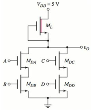
Figure 16.19 Figure for Exercise TYU 16.6
Expert Solution & Answer
Want to see the full answer?
Check out a sample textbook solution
Students have asked these similar questions
A certain digital circuits designed to operate with
voltage levels of -0.2Vdc and -3.0Vdc.
If H= 1 =-0.2 Vdc and L =0 =-3.0 Vdc, is this
positive logic or negative logic ?
H=+5.0Vdc. and. L=+1.0Vdc What are the
voltage levels between fall and rise times are
measured?
What is the value of Duty cycle H if the waveform
is high for 2 ms and low for 5 ms?
Assume Vth = 1V and k = 50mA/V2. Given the schematic below, do the following:
1) Indicate and verify the state of each MOSFET and ?0 for the following input combinations. Fill-out the table below for each assumed state of the MOSFET for every input combination. Use ?ds,on approximation for linear operation.
2) Determine what kind of logic circuit is implemented in the circuit.
Using the sine PWM method with the full bridge inverter below, it is desired to generate a voltage of 50 Hz on the serial RL load. A voltage of 120 V DC is applied to the input of the inverter circuit. Amplitude modulation rate ma -0.9 and frequency modulation rate mf -19. The resistance of the series RL load is 15 OHM and the coil inductance is 40 mH.
a) What is the power drawn by the load resistor?b) What is the total harmonic distortion value (THD) of the load current?
Chapter 16 Solutions
Microelectronics: Circuit Analysis and Design
Ch. 16 - Consider the NMOS inverter with resistor load in...Ch. 16 - The enhancementload NMOS inverter in Figure...Ch. 16 - Prob. 16.3EPCh. 16 - Prob. 16.4EPCh. 16 - Consider the NMOS inverter with enhancement load,...Ch. 16 - Prob. 16.2TYUCh. 16 - (a) Consider the results of Exercise Ex 16.1....Ch. 16 - Prob. 16.5EPCh. 16 - Prob. 16.6EPCh. 16 - (a) Design a threeinput NMOS NOR Logic gate with...
Ch. 16 - Consider the NMOS logic circuit in Figure 16.18....Ch. 16 - Repeat Exercise TYU 16.5 for the NMOS logic...Ch. 16 - The CMOS inverter in Figure 16.21 is biased at...Ch. 16 - swA CMOS inverter is biased at VDD=3V . The...Ch. 16 - A CMOS inverter is biased at VDD=1.8V . The...Ch. 16 - Prob. 16.7TYUCh. 16 - Repeat Exercise Ex 16.9 for a CMOS inverter biased...Ch. 16 - Determine the transistor sizes of a 3input CMOS...Ch. 16 - Design the widthtolength ratios of the transistors...Ch. 16 - Design a static CMOS logic circuit that implements...Ch. 16 - Prob. 16.10TYUCh. 16 - Prob. 16.11TYUCh. 16 - Sketch a clocked CMOS logic circuit that realizes...Ch. 16 - Prob. 16.12EPCh. 16 - Prob. 16.13TYUCh. 16 - Consider the CMOS transmission gate in Figure...Ch. 16 - Prob. 16.15TYUCh. 16 - Prob. 16.14EPCh. 16 - Prob. 16.16TYUCh. 16 - Prob. 16.17TYUCh. 16 - Sketch the quasistatic voltage transfer...Ch. 16 - Sketch an NMOS threeinput NOR logic gate. Describe...Ch. 16 - Discuss how more sophisticated (compared to the...Ch. 16 - Sketch the quasistatic voltage transfer...Ch. 16 - Discuss the parameters that affect the switching...Ch. 16 - Prob. 6RQCh. 16 - Sketch a CMOS threeinput NAND logic gate. Describe...Ch. 16 - sDiscuss how more sophisticated (compared to the...Ch. 16 - Prob. 9RQCh. 16 - Sketch an NMOS transmission gate and describe its...Ch. 16 - Sketch a CMOS transmission gate and describe its...Ch. 16 - Discuss what is meant by pass transistor logic.Ch. 16 - Prob. 13RQCh. 16 - Prob. 14RQCh. 16 - Prob. 15RQCh. 16 - Describe the basic architecture of a semiconductor...Ch. 16 - ‘Sketch a CMOS SRAM cell and describe its...Ch. 16 - Prob. 18RQCh. 16 - Describe a maskprogrammed MOSFET ROM memory.Ch. 16 - Describe the basic operation of a floating gate...Ch. 16 - Prob. 16.1PCh. 16 - Prob. 16.2PCh. 16 - (a) Redesign the resistive load inverter in Figure...Ch. 16 - Prob. D16.4PCh. 16 - Prob. 16.5PCh. 16 - Prob. D16.6PCh. 16 - Prob. 16.7PCh. 16 - Prob. 16.8PCh. 16 - For the depletion load inverter shown in Figure...Ch. 16 - Prob. 16.10PCh. 16 - Prob. D16.11PCh. 16 - Prob. D16.12PCh. 16 - Prob. 16.13PCh. 16 - For the two inverters in Figure P16.14, assume...Ch. 16 - Prob. 16.15PCh. 16 - Prob. 16.16PCh. 16 - Prob. 16.17PCh. 16 - Prob. 16.18PCh. 16 - Prob. D16.19PCh. 16 - Prob. 16.20PCh. 16 - Prob. 16.21PCh. 16 - Prob. 16.22PCh. 16 - In the NMOS circuit in Figure P16.23, the...Ch. 16 - Prob. 16.24PCh. 16 - Prob. 16.25PCh. 16 - Prob. 16.26PCh. 16 - What is the logic function implemented by the...Ch. 16 - Prob. D16.28PCh. 16 - Prob. D16.29PCh. 16 - Prob. 16.31PCh. 16 - Prob. 16.32PCh. 16 - Prob. 16.33PCh. 16 - Consider the CMOS inverter pair in Figure P16.34....Ch. 16 - Prob. 16.35PCh. 16 - Prob. 16.36PCh. 16 - Prob. 16.37PCh. 16 - Prob. 16.38PCh. 16 - Prob. 16.39PCh. 16 - (a) A CMOS digital logic circuit contains the...Ch. 16 - Prob. 16.41PCh. 16 - Prob. 16.42PCh. 16 - Prob. 16.43PCh. 16 - Prob. 16.44PCh. 16 - Prob. 16.45PCh. 16 - Prob. 16.46PCh. 16 - Prob. 16.47PCh. 16 - Prob. 16.48PCh. 16 - Prob. 16.49PCh. 16 - Prob. 16.50PCh. 16 - Prob. 16.51PCh. 16 - Prob. 16.52PCh. 16 - Prob. D16.53PCh. 16 - Figure P16.54 is a classic CMOS logic gate. (a)...Ch. 16 - Figure P16.55 is a classic CMOS logic gate. (a)...Ch. 16 - Consider the classic CMOS logic circuit in Figure...Ch. 16 - (a) Given inputs A,B,C,A,B and C , design a CMOS...Ch. 16 - (a) Given inputs A, B, C, D, and E, design a CMOS...Ch. 16 - (a) Determine the logic function performed by the...Ch. 16 - Prob. D16.60PCh. 16 - Prob. 16.61PCh. 16 - Prob. 16.62PCh. 16 - Sketch a clocked CMOS domino logic circuit that...Ch. 16 - Sketch a clocked CMOS domino logic circuit that...Ch. 16 - Prob. D16.65PCh. 16 - Prob. 16.66PCh. 16 - Prob. 16.67PCh. 16 - The NMOS transistors in the circuit shown in...Ch. 16 - Prob. 16.69PCh. 16 - Prob. 16.70PCh. 16 - Prob. 16.71PCh. 16 - (a) Design an NMOS pass transistor logic circuit...Ch. 16 - Prob. 16.73PCh. 16 - What is the logic function implemented by the...Ch. 16 - Prob. 16.75PCh. 16 - Prob. 16.76PCh. 16 - Prob. 16.77PCh. 16 - Consider the NMOS RS flipflop in Figure 16.63...Ch. 16 - Prob. 16.79PCh. 16 - Consider the circuit in Figure P16.80. Determine...Ch. 16 - Prob. D16.81PCh. 16 - Prob. 16.82PCh. 16 - Prob. 16.83PCh. 16 - Prob. 16.84PCh. 16 - (a) A 1 megabit memory is organized in a square...Ch. 16 - Prob. 16.86PCh. 16 - Prob. 16.87PCh. 16 - Prob. 16.88PCh. 16 - Prob. D16.89PCh. 16 - Prob. 16.90PCh. 16 - Prob. 16.91PCh. 16 - Prob. 16.92PCh. 16 - Prob. D16.93PCh. 16 - Prob. D16.94PCh. 16 - Prob. D16.95PCh. 16 - An analog signal in the range 0 to 5 V is to be...Ch. 16 - Prob. 16.97PCh. 16 - Prob. 16.98PCh. 16 - Prob. 16.99PCh. 16 - The weightedresistor D/A converter in Figure 16.90...Ch. 16 - The Nbit D/A converter with an R2R ladder network...Ch. 16 - Prob. 16.102PCh. 16 - Prob. 16.103PCh. 16 - Prob. 16.104PCh. 16 - Prob. 16.105PCh. 16 - Design a classic CMOS logic circuit that will...Ch. 16 - Prob. D16.111DPCh. 16 - Prob. D16.112DPCh. 16 - Prob. D16.113DP
Knowledge Booster


Learn more about
Need a deep-dive on the concept behind this application? Look no further. Learn more about this topic, electrical-engineering and related others by exploring similar questions and additional content below.Similar questions
- A full-bridge inverter has a switching sequence that produces a square wave voltage across a series RL load. The switching frequency is 60 Hz, Vdc=100 V, R equals to 10 Ohm, and L equals 25 mH. The average current in the dc source is. Select one: O a. 52 A O b. None of the above O c. 4.41 A O d. 300 Aarrow_forward(a) Discuss the key characteristics of Unipolar Logic Families and Bipolar Logic Families. What points are important to consider for interfacing the components from different Logic Families.arrow_forward2. a) Compare and differentiate a single phase full bridge inverter with a single phase full bridge rectifier in terms of construction and operation. Discuss how the switching operation of the inverter can effect the output waveform and total. harmonics distortion (THD) value.. Use suitable diagram for better explanation.arrow_forward
- Diode Logic Gates - OR, NOR, AND, Not, & NAND Circuit diagram and explain itarrow_forwardUsing the sine PWM method with the full bridge inverter below, it is desired to generate a voltage of 50Hz on the series RL load. A voltage of 120 V DC is applied to the input of the inverter circuit. Amplitude modulation rate ma = 0.9 and frequency modulation rate mj = 19. The resistance of the series RL load is 15 ohms and the coil inductance is 40 mH. What is the total harmonic distortion value (THD) of the power drawn by the load resistor and the load current?arrow_forward(a) Construct an Inverter Logic Gate using both TTL and CMOS Logic Family.arrow_forward
- Q4: Suggest a control gate drive circuit for a Triac, which is used to control a fan regulator. The gate signals should be synchronized with the input voltage. Draw the complete: 1. Circuit diagram with the load and 2. The waveform of the input and output voltages. ) Q.13 Indicate whether the following statements are correct or not then correct the incorrect statements 1) the multi pulse selected notching technique used in inverter is used to eliminate the low order harmonics and to reduce switching frequency, 2) In 3-phase half-controlled half-wave rectifier, the firing angle can be varied from 0 to 180 degrees while in 6-phase half-controlled half-wave rectifier can be varied from 0 to 150 degrees Q.14 Indicate whether the following statements are correct or not then correct the incorrect statements 1) In rectifier circuits, lower pulse number and connecting either primary or secondary of 3- phase winding in delta will reduce the harmonics content of the drawr. current 2) In…arrow_forwardWhat are the disadvantages of ratioed NMOS logic circuits?arrow_forward(e) Describe, with the help of sketches, the definition and meaning of noise margins in an inverter logic gate.arrow_forward
- 3. PWM Inverter The full bridge inverter is used to produce a 60 Hz voltage across a series R-L load using bipolar PWM. The dc input to the bridge is 100 V, the amplitude modulation ratio ma is 0.8 and the frequency modulation ratio m, is 21. The load has a resistance of R = 10n and a 20mH. Determine the a) the amplitude of the 60-Hz component of the output voltage and load current b) power absorbed by the load resistor c) THD of load series inductance of L current. m,=1 0.9 0.8 0.7 0.6 0.5 0.4 0.3 0.2 0.1 1.00 0.90 0.80 0.70 0.60 0.50 0.40 0.10 0.30 1.20 0.20 1.24 n=1 0.60 0.71 0.82 0.92 1.01 1.08 1.15 1.27 n=m, n=mf±2 0.32 0.27 0.22 0.17 0.13 0.09 0.06 0.03 0.02 0.00arrow_forwardSketch the VTC for a logic inverter with VoH = 5 V, Vol = 0.2 V, V.IL= 1.4 V, and VIH= 1.6 V. Also, determine the logic swing , transition width, and the noise margins.arrow_forwardDraw the circuit diagram of 4-bit Ripple Carry Adder. Page 6 of 8arrow_forward
arrow_back_ios
SEE MORE QUESTIONS
arrow_forward_ios
Recommended textbooks for you
 Introductory Circuit Analysis (13th Edition)Electrical EngineeringISBN:9780133923605Author:Robert L. BoylestadPublisher:PEARSON
 Delmar's Standard Textbook Of ElectricityElectrical EngineeringISBN:9781337900348Author:Stephen L. HermanPublisher:Cengage Learning
 Programmable Logic ControllersElectrical EngineeringISBN:9780073373843Author:Frank D. PetruzellaPublisher:McGraw-Hill Education
 Fundamentals of Electric CircuitsElectrical EngineeringISBN:9780078028229Author:Charles K Alexander, Matthew SadikuPublisher:McGraw-Hill Education
 Electric Circuits. (11th Edition)Electrical EngineeringISBN:9780134746968Author:James W. Nilsson, Susan RiedelPublisher:PEARSON
 Engineering ElectromagneticsElectrical EngineeringISBN:9780078028151Author:Hayt, William H. (william Hart), Jr, BUCK, John A.Publisher:Mcgraw-hill Education,
Introductory Circuit Analysis (13th Edition)
Electrical Engineering
ISBN:9780133923605
Author:Robert L. Boylestad
Publisher:PEARSON
Delmar's Standard Textbook Of Electricity
Electrical Engineering
ISBN:9781337900348
Author:Stephen L. Herman
Publisher:Cengage Learning
Programmable Logic Controllers
Electrical Engineering
ISBN:9780073373843
Author:Frank D. Petruzella
Publisher:McGraw-Hill Education
Fundamentals of Electric Circuits
Electrical Engineering
ISBN:9780078028229
Author:Charles K Alexander, Matthew Sadiku
Publisher:McGraw-Hill Education
Electric Circuits. (11th Edition)
Electrical Engineering
ISBN:9780134746968
Author:James W. Nilsson, Susan Riedel
Publisher:PEARSON
Engineering Electromagnetics
Electrical Engineering
ISBN:9780078028151
Author:Hayt, William H. (william Hart), Jr, BUCK, John A.
Publisher:Mcgraw-hill Education,
CMOS Tech: NMOS and PMOS Transistors in CMOS Inverter (3-D View); Author: G Chang;https://www.youtube.com/watch?v=oSrUsM0hoPs;License: Standard Youtube License