
Microelectronics: Circuit Analysis and Design
4th Edition
ISBN: 9780073380643
Author: Donald A. Neamen
Publisher: McGraw-Hill Companies, The
expand_more
expand_more
format_list_bulleted
Videos
Textbook Question
Chapter 16, Problem 16.59P
(a) Determine the logic function performed by the circuit in Figure P16.59. (b) Determine the W/L ratios to provide symmetrical switching times equal to the basic CMOS inverter with
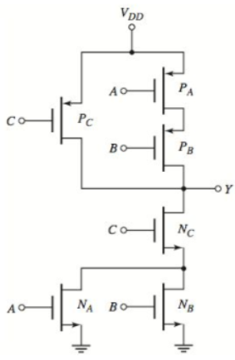
Figure P16.59
Expert Solution & Answer
Want to see the full answer?
Check out a sample textbook solution
Students have asked these similar questions
(a) Construct an Inverter Logic Gate using both TTL and CMOS Logic Family.
a) A standard TTL inverter gate is shown in the figure. The supply voltage is 5V. Calculate the
output voltage for both logic low and logic high input cases assuming input voltages
respectively as 0.11V and 4.2V.
Br= 130; BR = 0.24. You can make approximations when needed.
Br = IcIs active region; BR = IE/ls inverse active region
b) Assume you connect a resistor of 1.8K to the output of the circuit when the output is at logic
high. What will be the change in the output voltage?
1302
R3
1.6k2
R,
4k2
Input o
T,
Output
T,
V,
V.
IkQ
R,
Design an asymmetrical inverter to meet the delay specificationa symmetrical CMOS reference inverter to provide a delay of 1 ns when driving a 10-pF load.(a) Assume VDD =2.5 V. (b) Assume VDD =1.8 V and VT N =−VT P =0.45 V. with (W/L)P = 2(W/L)N .
Chapter 16 Solutions
Microelectronics: Circuit Analysis and Design
Ch. 16 - Consider the NMOS inverter with resistor load in...Ch. 16 - The enhancementload NMOS inverter in Figure...Ch. 16 - Prob. 16.3EPCh. 16 - Prob. 16.4EPCh. 16 - Consider the NMOS inverter with enhancement load,...Ch. 16 - Prob. 16.2TYUCh. 16 - (a) Consider the results of Exercise Ex 16.1....Ch. 16 - Prob. 16.5EPCh. 16 - Prob. 16.6EPCh. 16 - (a) Design a threeinput NMOS NOR Logic gate with...
Ch. 16 - Consider the NMOS logic circuit in Figure 16.18....Ch. 16 - Repeat Exercise TYU 16.5 for the NMOS logic...Ch. 16 - The CMOS inverter in Figure 16.21 is biased at...Ch. 16 - swA CMOS inverter is biased at VDD=3V . The...Ch. 16 - A CMOS inverter is biased at VDD=1.8V . The...Ch. 16 - Prob. 16.7TYUCh. 16 - Repeat Exercise Ex 16.9 for a CMOS inverter biased...Ch. 16 - Determine the transistor sizes of a 3input CMOS...Ch. 16 - Design the widthtolength ratios of the transistors...Ch. 16 - Design a static CMOS logic circuit that implements...Ch. 16 - Prob. 16.10TYUCh. 16 - Prob. 16.11TYUCh. 16 - Sketch a clocked CMOS logic circuit that realizes...Ch. 16 - Prob. 16.12EPCh. 16 - Prob. 16.13TYUCh. 16 - Consider the CMOS transmission gate in Figure...Ch. 16 - Prob. 16.15TYUCh. 16 - Prob. 16.14EPCh. 16 - Prob. 16.16TYUCh. 16 - Prob. 16.17TYUCh. 16 - Sketch the quasistatic voltage transfer...Ch. 16 - Sketch an NMOS threeinput NOR logic gate. Describe...Ch. 16 - Discuss how more sophisticated (compared to the...Ch. 16 - Sketch the quasistatic voltage transfer...Ch. 16 - Discuss the parameters that affect the switching...Ch. 16 - Prob. 6RQCh. 16 - Sketch a CMOS threeinput NAND logic gate. Describe...Ch. 16 - sDiscuss how more sophisticated (compared to the...Ch. 16 - Prob. 9RQCh. 16 - Sketch an NMOS transmission gate and describe its...Ch. 16 - Sketch a CMOS transmission gate and describe its...Ch. 16 - Discuss what is meant by pass transistor logic.Ch. 16 - Prob. 13RQCh. 16 - Prob. 14RQCh. 16 - Prob. 15RQCh. 16 - Describe the basic architecture of a semiconductor...Ch. 16 - ‘Sketch a CMOS SRAM cell and describe its...Ch. 16 - Prob. 18RQCh. 16 - Describe a maskprogrammed MOSFET ROM memory.Ch. 16 - Describe the basic operation of a floating gate...Ch. 16 - Prob. 16.1PCh. 16 - Prob. 16.2PCh. 16 - (a) Redesign the resistive load inverter in Figure...Ch. 16 - Prob. D16.4PCh. 16 - Prob. 16.5PCh. 16 - Prob. D16.6PCh. 16 - Prob. 16.7PCh. 16 - Prob. 16.8PCh. 16 - For the depletion load inverter shown in Figure...Ch. 16 - Prob. 16.10PCh. 16 - Prob. D16.11PCh. 16 - Prob. D16.12PCh. 16 - Prob. 16.13PCh. 16 - For the two inverters in Figure P16.14, assume...Ch. 16 - Prob. 16.15PCh. 16 - Prob. 16.16PCh. 16 - Prob. 16.17PCh. 16 - Prob. 16.18PCh. 16 - Prob. D16.19PCh. 16 - Prob. 16.20PCh. 16 - Prob. 16.21PCh. 16 - Prob. 16.22PCh. 16 - In the NMOS circuit in Figure P16.23, the...Ch. 16 - Prob. 16.24PCh. 16 - Prob. 16.25PCh. 16 - Prob. 16.26PCh. 16 - What is the logic function implemented by the...Ch. 16 - Prob. D16.28PCh. 16 - Prob. D16.29PCh. 16 - Prob. 16.31PCh. 16 - Prob. 16.32PCh. 16 - Prob. 16.33PCh. 16 - Consider the CMOS inverter pair in Figure P16.34....Ch. 16 - Prob. 16.35PCh. 16 - Prob. 16.36PCh. 16 - Prob. 16.37PCh. 16 - Prob. 16.38PCh. 16 - Prob. 16.39PCh. 16 - (a) A CMOS digital logic circuit contains the...Ch. 16 - Prob. 16.41PCh. 16 - Prob. 16.42PCh. 16 - Prob. 16.43PCh. 16 - Prob. 16.44PCh. 16 - Prob. 16.45PCh. 16 - Prob. 16.46PCh. 16 - Prob. 16.47PCh. 16 - Prob. 16.48PCh. 16 - Prob. 16.49PCh. 16 - Prob. 16.50PCh. 16 - Prob. 16.51PCh. 16 - Prob. 16.52PCh. 16 - Prob. D16.53PCh. 16 - Figure P16.54 is a classic CMOS logic gate. (a)...Ch. 16 - Figure P16.55 is a classic CMOS logic gate. (a)...Ch. 16 - Consider the classic CMOS logic circuit in Figure...Ch. 16 - (a) Given inputs A,B,C,A,B and C , design a CMOS...Ch. 16 - (a) Given inputs A, B, C, D, and E, design a CMOS...Ch. 16 - (a) Determine the logic function performed by the...Ch. 16 - Prob. D16.60PCh. 16 - Prob. 16.61PCh. 16 - Prob. 16.62PCh. 16 - Sketch a clocked CMOS domino logic circuit that...Ch. 16 - Sketch a clocked CMOS domino logic circuit that...Ch. 16 - Prob. D16.65PCh. 16 - Prob. 16.66PCh. 16 - Prob. 16.67PCh. 16 - The NMOS transistors in the circuit shown in...Ch. 16 - Prob. 16.69PCh. 16 - Prob. 16.70PCh. 16 - Prob. 16.71PCh. 16 - (a) Design an NMOS pass transistor logic circuit...Ch. 16 - Prob. 16.73PCh. 16 - What is the logic function implemented by the...Ch. 16 - Prob. 16.75PCh. 16 - Prob. 16.76PCh. 16 - Prob. 16.77PCh. 16 - Consider the NMOS RS flipflop in Figure 16.63...Ch. 16 - Prob. 16.79PCh. 16 - Consider the circuit in Figure P16.80. Determine...Ch. 16 - Prob. D16.81PCh. 16 - Prob. 16.82PCh. 16 - Prob. 16.83PCh. 16 - Prob. 16.84PCh. 16 - (a) A 1 megabit memory is organized in a square...Ch. 16 - Prob. 16.86PCh. 16 - Prob. 16.87PCh. 16 - Prob. 16.88PCh. 16 - Prob. D16.89PCh. 16 - Prob. 16.90PCh. 16 - Prob. 16.91PCh. 16 - Prob. 16.92PCh. 16 - Prob. D16.93PCh. 16 - Prob. D16.94PCh. 16 - Prob. D16.95PCh. 16 - An analog signal in the range 0 to 5 V is to be...Ch. 16 - Prob. 16.97PCh. 16 - Prob. 16.98PCh. 16 - Prob. 16.99PCh. 16 - The weightedresistor D/A converter in Figure 16.90...Ch. 16 - The Nbit D/A converter with an R2R ladder network...Ch. 16 - Prob. 16.102PCh. 16 - Prob. 16.103PCh. 16 - Prob. 16.104PCh. 16 - Prob. 16.105PCh. 16 - Design a classic CMOS logic circuit that will...Ch. 16 - Prob. D16.111DPCh. 16 - Prob. D16.112DPCh. 16 - Prob. D16.113DP
Knowledge Booster


Learn more about
Need a deep-dive on the concept behind this application? Look no further. Learn more about this topic, electrical-engineering and related others by exploring similar questions and additional content below.Similar questions
- Implement logic function shown below with static CMOS gate. Out = ABC + ĀB + BC + ACarrow_forwardBriefly describe the internal and external control of inverters.arrow_forwardR. Convert the following octal numbers to binary: (a) 468 (b) 7238 Q. The input waveforms applied to a 4-input AND gate are as indicated in Figure 1. The output of the AND gate is fed to an inverter. Draw the net output waveform of this system. 4900arrow_forward
- What is the power-delay product for a symmetrical CMOSinverter with (W/L)N = 2/1, (W/L)P = 5/1,VDD = 2.5 V, and C = 0.3 pF? (b) Repeat forVDD = 2.0 V. (c) Repeat for VDD = 1.8 V.? How much power does the inverter dissipate if it is switching at a frequency of 100 MHz?arrow_forward(a) Figure Q.4 (a) shows a combinational logic cireuit with output, Z and Table Q.4(a) depicts the delay for each logic gate in nanoseconds (ns). Determine the critical path and critical path delay in nanoseconds (ns). В Figure Q.4(a) Table Q.4 (a) Logic Gate NOT Delay (ns) 4 OR 8 AND 16 NAND 12 NOR 10 XOR 28 XNOR 32arrow_forwardDescribe the functionality of a three-state inverter.arrow_forward
- (a) A CMOS inverter has (W/L)N =15/1,(W/L)P =15/1, and VDD =3.3V. What is the peakcurrent in the logic gate and at what input voltagedoes it occur? (b) Repeat for VDD =2.5 V.arrow_forwardUsing the sine PWM method with the full bridge inverter below, it is desired to generate a voltage of 50 Hz on the serial RL load. A voltage of 120 V DC is applied to the input of the inverter circuit. Amplitude modulation rate ma -0.9 and frequency modulation rate mf -19. The resistance of the series RL load is 15 OHM and the coil inductance is 40 mH. a) What is the power drawn by the load resistor?b) What is the total harmonic distortion value (THD) of the load current?arrow_forward7) The following figure shows a transistor-level (CMOS) circuit for some logic gate. Sketch the logic gate for the CMOS gate. Choices: a) NAND gate b) AND gate c) OR gate d) NOR gatearrow_forward
- e) Explain the terms VSC and ISC. f) Explain the applications of DC-Link invertes. g) Explain the differences of Half and Full Bridge inverters.arrow_forwardAssume Vth = 1V and k = 50mA/V2. Given the schematic below, do the following: 1) Indicate and verify the state of each MOSFET and ?0 for the following input combinations. Fill-out the table below for each assumed state of the MOSFET for every input combination. Use ?ds,on approximation for linear operation. 2) Determine what kind of logic circuit is implemented in the circuit.arrow_forward(a) What is the power-delay product for a symmetrical CMOS inverterwith (W/L)N =2/1, (W/L)P =5/1, C =0.25 pF,VDD =3.3 V, VTN =0.75 V, and VTP =−0.75 V? (b) Estimate the maximum switchingfrequency for this inverter. (c) Howmuch powerdoes the inverter dissipate if it is switching at thefrequency found in (b)?arrow_forward
arrow_back_ios
SEE MORE QUESTIONS
arrow_forward_ios
Recommended textbooks for you
 Introductory Circuit Analysis (13th Edition)Electrical EngineeringISBN:9780133923605Author:Robert L. BoylestadPublisher:PEARSON
 Delmar's Standard Textbook Of ElectricityElectrical EngineeringISBN:9781337900348Author:Stephen L. HermanPublisher:Cengage Learning
 Programmable Logic ControllersElectrical EngineeringISBN:9780073373843Author:Frank D. PetruzellaPublisher:McGraw-Hill Education
 Fundamentals of Electric CircuitsElectrical EngineeringISBN:9780078028229Author:Charles K Alexander, Matthew SadikuPublisher:McGraw-Hill Education
 Electric Circuits. (11th Edition)Electrical EngineeringISBN:9780134746968Author:James W. Nilsson, Susan RiedelPublisher:PEARSON
 Engineering ElectromagneticsElectrical EngineeringISBN:9780078028151Author:Hayt, William H. (william Hart), Jr, BUCK, John A.Publisher:Mcgraw-hill Education,
Introductory Circuit Analysis (13th Edition)
Electrical Engineering
ISBN:9780133923605
Author:Robert L. Boylestad
Publisher:PEARSON
Delmar's Standard Textbook Of Electricity
Electrical Engineering
ISBN:9781337900348
Author:Stephen L. Herman
Publisher:Cengage Learning
Programmable Logic Controllers
Electrical Engineering
ISBN:9780073373843
Author:Frank D. Petruzella
Publisher:McGraw-Hill Education
Fundamentals of Electric Circuits
Electrical Engineering
ISBN:9780078028229
Author:Charles K Alexander, Matthew Sadiku
Publisher:McGraw-Hill Education
Electric Circuits. (11th Edition)
Electrical Engineering
ISBN:9780134746968
Author:James W. Nilsson, Susan Riedel
Publisher:PEARSON
Engineering Electromagnetics
Electrical Engineering
ISBN:9780078028151
Author:Hayt, William H. (william Hart), Jr, BUCK, John A.
Publisher:Mcgraw-hill Education,
Diode Logic Gates - OR, NOR, AND, & NAND; Author: The Organic Chemistry Tutor;https://www.youtube.com/watch?v=9lqwSaIDm2g;License: Standard Youtube License