
Concept explainers
Videos
For the two inverters in Figure P16.14, assume
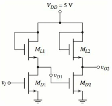
Figure P16.14
Want to see the full answer?
Check out a sample textbook solution
Chapter 16 Solutions
Microelectronics: Circuit Analysis and Design


- A new floating point representation is proposed so that implicit normalization to the mantissa and biased exponent. The representation is similar to that of IEEE 754 format i.e., Bias = (2k - 1) because it is %3D used to represent + 0, t oo. Let 4 bit biased exponent and, 7-bit mantissa is placed in 12 bit register as shown below. E (4) Which of the following pattern denote the value 14.25?arrow_forwardThe load voltage waveform of a single phase full bridge inverter supplied from 30OV DC voltage source is shown in below figure. Output frequency is 50HZ and the load consists of series R-L components. The load vahues are 22 and 0.04H, respectively. (Conduction interval for half period is 120°) 150 100 50 T -50 3 -100 -150 .002 .004 .006 008 .01 .012 .014 .016 .018 .02 Time (sec) a. Calculate and draw the load current for the first two-period interval b. Calculate and draw the load current for the steady-state condition c. Find the RMS values of the load voltage and the load current d Calculate and draw the voltage across the load inductance e. Calculate and draw the source current and find its average vahuearrow_forwardDraw the figure for memory segments with 8086 microprocessor software model. Explain the logical address structure used for each segment (Explain which registers are used in logical address presentation of each segment; segment address : offset address). Give an example solution to find the physical address in a segment from the logical address for 8086 microprocessor.arrow_forward
- The output voltage and current wave forms of single phase full bridge voltage source inverter with R - L load is shown. Where R = 2002, L = 0.2H. It is operated without PWM and fs = 100 Hz. The zero crossing instant is (a) 1.63 ms (b) 2.19 ms (c) 2.25 ms (d) 2.72 ms M +400V -400Varrow_forwardThe load voltage waveform of a single phase full bridge inverter supplied from 300V DC voltage source is shown in below figure. Output frequency is 50HZ and the load consists of series R-L components. The load values are 2N and 0.04H, respectively. (Conduction interval for half period is 120°) 150 100 50 T -50 3 -100 -150 .002 .004 .006 .008 .014 ,02 .01 Time (sec) .012 .016 .018 a. Find the RMS values of the load voltage and the load current b. Calculate and draw the voltage across the load inductance c. Calculate and draw the source current and find its average valuearrow_forwardUsing the sine PWM method with the full bridge inverter below, it is desired to generate a voltage of 50 Hz on the serial RL load. A voltage of 120 V DC is applied to the input of the inverter circuit. Amplitude modulation rate ma -0.9 and frequency modulation rate mf -19. The resistance of the series RL load is 15 OHM and the coil inductance is 40 mH. a) What is the power drawn by the load resistor?b) What is the total harmonic distortion value (THD) of the load current?arrow_forward
- 3. PWM Inverter The full bridge inverter is used to produce a 60 Hz voltage across a series R-L load using bipolar PWM. The dc input to the bridge is 100 V, the amplitude modulation ratio ma is 0.8 and the frequency modulation ratio m, is 21. The load has a resistance of R = 10n and a 20mH. Determine the a) the amplitude of the 60-Hz component of the output voltage and load current b) power absorbed by the load resistor c) THD of load series inductance of L current. m,=1 0.9 0.8 0.7 0.6 0.5 0.4 0.3 0.2 0.1 1.00 0.90 0.80 0.70 0.60 0.50 0.40 0.10 0.30 1.20 0.20 1.24 n=1 0.60 0.71 0.82 0.92 1.01 1.08 1.15 1.27 n=m, n=mf±2 0.32 0.27 0.22 0.17 0.13 0.09 0.06 0.03 0.02 0.00arrow_forwardUsing Table 16.1 , identify the components of the logic system shown in the figure.arrow_forwardQuestion- A single phase full bridge inverter controls the power in a resistive load by uniform multiple pulse modulation. The frequency of triangular carrier wave is 1kHz and inverter reference wave frequency is 125Hz. If the total pulse width is 120°, find the width of each pulse?arrow_forward
- 1. If the input of an inverter is connected to a square wave, what will be present on the output? A. A constant logic high B. A constant logic low C. A sine wave D. A square wave that mirrors the input square wave 2. Assume that one input of a two-input AND gate is connected to a square wave. If the other input is connected to a logic high, what will be present on the output? A. A constant logic high B. A square wave C. A square wave that mirrors the input square wave D. A constant logic lowarrow_forwardAn inverter with a resistive load, VDD = 3.3 V, P = 0.1 mW, VL = 0.2 V, K'n = 60 UA/V2 and VT N = 0.75 V. The value of (W/L)S is:arrow_forward(b) For a gated S-R latch. determine the Q output for the inputs in the following Figure. Show it in proper relation to the enable input, also draw the input waveforms on your answer script. Assume that Q starts LOW. EN S R Minimize the combinational logic circuit in the following figure using Karnaugh's map only. Inverters for the complemented variables are not shown. Q2.arrow_forward
 Introductory Circuit Analysis (13th Edition)Electrical EngineeringISBN:9780133923605Author:Robert L. BoylestadPublisher:PEARSON
 Delmar's Standard Textbook Of ElectricityElectrical EngineeringISBN:9781337900348Author:Stephen L. HermanPublisher:Cengage Learning
 Programmable Logic ControllersElectrical EngineeringISBN:9780073373843Author:Frank D. PetruzellaPublisher:McGraw-Hill Education
 Fundamentals of Electric CircuitsElectrical EngineeringISBN:9780078028229Author:Charles K Alexander, Matthew SadikuPublisher:McGraw-Hill Education
 Electric Circuits. (11th Edition)Electrical EngineeringISBN:9780134746968Author:James W. Nilsson, Susan RiedelPublisher:PEARSON
 Engineering ElectromagneticsElectrical EngineeringISBN:9780078028151Author:Hayt, William H. (william Hart), Jr, BUCK, John A.Publisher:Mcgraw-hill Education,