
Microelectronics: Circuit Analysis and Design
4th Edition
ISBN: 9780073380643
Author: Donald A. Neamen
Publisher: McGraw-Hill Companies, The
expand_more
expand_more
format_list_bulleted
Videos
Textbook Question
Chapter 7, Problem D7.20P
The transistor in the circuit in Figure P7.20 has parameters
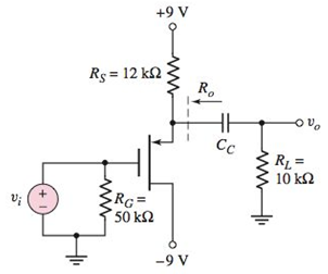
Figure P7.20
Expert Solution & Answer
Want to see the full answer?
Check out a sample textbook solution
Students have asked these similar questions
Q7. Figure Q7(a) shows the spectrum of a frequency modulated waveform with a sinusoidal
modulation.
12
4.8
5.0
5.2
5.4
5.6
5.8
6.0
Frequency/MHz
Figure Q7: (a) Spectrum of a frequency modulated waveform with a sinusoidal modulation.
(a) Is this modulated waveform described as narrowband or as wideband?
(b) What is the value of the carrier frequency?
(c) What is the value of the modulation frequency?
(d) Determine the value of the peak frequency deviation. Plots of Bessel functions of the
first kind are provided below in Figure Q7(b) to assist you.
(e) Estimate the fraction of the total signal power at the carrier frequency.
(f) Detection of such a frequency modulated signal is usually accomplished with the use
of a discriminator. Describe the function of a discriminator.
(g) What is the equivalent AM modulation index obtained if this signal in Figure Q7(a) is
demodulated with a high-pass RC filter discriminator?
J„(x)
1.0
0.8
0.6
0.4
0.2
-0.2
-0.4
Figure Q7: (b) Bessel functions of the…
Q2.
Consider the circuit shown in Figure P7.15. The transistor has parameters
B = 120 and VA
collector-emitter voltage is VCEO = 1.25 V. (a) Determine Rc, (b) find Ico,
and (c) determine the maximum gain.
= ∞. The circuit bandwidth is 800 MHz and the quiescent
Vcc= 2.5 V
RC
CL = 0.08 pF
Figure P7.15
(a) Design the circuit shown in Figure P7.18 such that Ipo = 0.8 mA,
VDsQ = 3.2 V, Rin
K, = 0.5 mA/V², VTN = 1.2 V, and A = 0. (b) What is the midband volt-
age gain? (c) Determine the magnitude of the voltage gain at (i) f = 5 Hz,
(ii) f = 14 Hz, and (iii) f = 25 Hz. (d) Sketch the Bode plot of the voltage
gain magnitude and phase.
160 k2, and fr
16 Hz. The transistor parameters are
ass
VDD =9 V
Rp
R1
Rin 1
O vO
Cc
Rs =
0.5 k2
R2
Figure P7.18
ww
ww
Chapter 7 Solutions
Microelectronics: Circuit Analysis and Design
Ch. 7 - (a) For the circuit shown in Figure 7.2, the...Ch. 7 - The circuit shown in Figure 7.10 has parameters of...Ch. 7 - For the equivalent circuit shown in Figure 7.13,...Ch. 7 - The equivalent circuit in Figure 7.14 has circuit...Ch. 7 - The parameters in the circuit shown in Figure 7.15...Ch. 7 - For the circuit shown in Figure 7.2 1(a), the...Ch. 7 - Consider the circuit shown in Figure 7.22(a). The...Ch. 7 - For the emitterfollower circuit shown in Figure...Ch. 7 - The circuit shown in Figure 7.27(a) has parameters...Ch. 7 - Consider the common-base circuit shown in Figure...
Ch. 7 - The commonemitter circuit shown in Figure 7.34...Ch. 7 - A bipolar transistor has parameters o=120 ,...Ch. 7 - Prob. 7.9EPCh. 7 - For the circuit in Figure 7.41(a), the parameters...Ch. 7 - A bipolar transistor is biased at ICQ=120A and its...Ch. 7 - For the transistor described in Example 7.9 and...Ch. 7 - The parameters of a bipolar transistor are: o=150...Ch. 7 - The parameters of an nchannel MOSFET are...Ch. 7 - For the circuit in Figure 7.55, the transistor...Ch. 7 - An nchannel MOSFET has parameters Kn=0.4mA/V2 ,...Ch. 7 - An nchannel MOSFET has a unitygain bandwidth of...Ch. 7 - For a MOSFET, assume that gm=1.2mA/V . The basic...Ch. 7 - The transistor in the circuit in Figure 7.60 has...Ch. 7 - Consider the commonbase circuit in Figure 7.64....Ch. 7 - The cascode circuit in Figure 7.65 has parameters...Ch. 7 - Prob. 7.12TYUCh. 7 - For the circuit in Figure 7.72, the transistor...Ch. 7 - Describe the general frequency response of an...Ch. 7 - Describe the general characteristics of the...Ch. 7 - Describe what is meant by a system transfer...Ch. 7 - What is the criterion that defines a corner, or...Ch. 7 - Describe what is meant by the phase of the...Ch. 7 - Describe the time constant technique for...Ch. 7 - Describe the general frequency response of a...Ch. 7 - Sketch the expanded hybrid model of the BJT.Ch. 7 - Prob. 9RQCh. 7 - Prob. 10RQCh. 7 - Prob. 11RQCh. 7 - Sketch the expanded smallsignal equivalent circuit...Ch. 7 - Define the cutoff frequency for a MOSFET.Ch. 7 - Prob. 14RQCh. 7 - Why is there not a Miller effect in a commonbase...Ch. 7 - Describe the configuration of a cascode amplifier.Ch. 7 - Why is the bandwidth of a cascode amplifier...Ch. 7 - Why is the bandwidth of the emitterfollower...Ch. 7 - Prob. 7.1PCh. 7 - Prob. 7.2PCh. 7 - Consider the circuit in Figure P7.3. (a) Derive...Ch. 7 - Consider the circuit in Figure P7.4 with a signal...Ch. 7 - Consider the circuit shown in Figure P7.5. (a)...Ch. 7 - A voltage transfer function is given by...Ch. 7 - Sketch the Bode magnitude plots for the following...Ch. 7 - (a) Determine the transfer function corresponding...Ch. 7 - Consider the circuit shown in Figure 7.15 with...Ch. 7 - For the circuit shown in Figure P7.12, the...Ch. 7 - The circuit shown in Figure 7.10 has parameters...Ch. 7 - The transistor shown in Figure P7.14 has...Ch. 7 - Consider the circuit shown in Figure P7.15. The...Ch. 7 - The transistor in the circuit shown in Figure...Ch. 7 - For the common-emitter circuit in Figure P7.17,...Ch. 7 - The transistor in the circuit in Figure P7.20 has...Ch. 7 - For the circuit in Figure P7.21, the transistor...Ch. 7 - (a) For the circuit shown in Figure P7.22, write...Ch. 7 - Consider the circuit shown in Figure P7.23. (a)...Ch. 7 - The parameters of the transistor in the circuit in...Ch. 7 - A capacitor is placed in parallel with RL in the...Ch. 7 - The parameters of the transistor in the circuit in...Ch. 7 - Prob. D7.27PCh. 7 - The circuit in Figure P7.28 is a simple output...Ch. 7 - Reconsider the circuit in Figure P728. The...Ch. 7 - Consider the circuit shown in Figure P7.32. The...Ch. 7 - The commonemitter circuit in Figure P7.35 has an...Ch. 7 - Consider the commonbase circuit in Figure 7.33 in...Ch. 7 - Prob. 7.39PCh. 7 - The parameters of the transistor in the circuit in...Ch. 7 - In the commonsource amplifier in Figure 7.25(a) in...Ch. 7 - A bipolar transistor has fT=4GHz , o=120 , and...Ch. 7 - A highfrequency bipolar transistor is biased at...Ch. 7 - (a) The frequency fT of a bipolar transistor is...Ch. 7 - The circuit in Figure P7.48 is a hybrid ...Ch. 7 - Consider the circuit in Figure P7.49. Calculate...Ch. 7 - A common-emitter equivalent circuit is shown in...Ch. 7 - For the common-emitter circuit in Figure 7.41(a)...Ch. 7 - For the commonemitter circuit in Figure P7.52,...Ch. 7 - Consider the circuit in Figure P7.52. The resistor...Ch. 7 - The parameters of the circuit shown in Figure...Ch. 7 - The parameters of an nchannel MOSFET are kn=80A/V2...Ch. 7 - Find fT for a MOSFET biased at IDQ=120A and...Ch. 7 - Fill in the missing parameter values in the...Ch. 7 - (a) An nchannel MOSFET has an electron mobility of...Ch. 7 - A commonsource equivalent circuit is shown in...Ch. 7 - Prob. 7.60PCh. 7 - The parameters of an ideal nchannel MOSFET are...Ch. 7 - Figure P7.62 shows the highfrequency equivalent...Ch. 7 - For the FET circuit in Figure P7.63, the...Ch. 7 - The midband voltage gain of a commonsource MOSFET...Ch. 7 - Prob. 7.65PCh. 7 - Prob. 7.67PCh. 7 - The bias voltages of the circuit shown in Figure...Ch. 7 - For the PMOS commonsource circuit shown in Figure...Ch. 7 - In the commonbase circuit shown in Figure P7.70,...Ch. 7 - Repeat Problem 7.70 for the commonbase circuit in...Ch. 7 - In the commongate circuit in Figure P7.72, the...
Knowledge Booster


Learn more about
Need a deep-dive on the concept behind this application? Look no further. Learn more about this topic, electrical-engineering and related others by exploring similar questions and additional content below.Similar questions
- Q5. In the circuit in Figure P7.65, the transistor parameters are: B = 120, VBE (on) = 0.7 V, VA = 100 V, C, = 1 pF, and fr = 600 MHz. (a) Deter- mine C and the equivalent Miller capacitance CM. State any approxima- tions or assumptions that you make. (b) Find the upper 3 dB frequency and the midband voltage gain. +5 V Rc=4 k2 R = 33 k2 HH Cc2 = 2 µF CCi = 1 µF wwH Rs=2 kQ RL = 5 k2 R2 = 22 kO RE= 4 k2 CE= 10 µF Figure P7.65arrow_forward7.65 In the circuit in Figure P7.65, the transistor parameters are: B 120, Ver(on)=0.7 V, VA 100 V, C -I pF, and fr mine C, and the equivalent Miller capacitance Cy. State any approxima- tions or assumptions that you make. (b) Find the upper 3 dB frequency and the midband voltage gain. -600 MHz. (a) Deter- +5 V R= 33 ka wwHH Ry=22 k2 4 k2 10 wwarrow_forwardQ7. For the PMOS common-source circuit shown in Figure P7.69, the transistor parameters are: VTp = -2 V, K, Cgd = 3 pF. (a) Determine the upper 3 dB frequency. (b) What is the equiv- alent Miller capacitance? State any assumptions or approximations that you make. (c) Find the midband voltage gain. 1 mA/V², 1 = 0, Cgs = 15 pF, and +10 V Rs 0.5 kQ R=8 k2 Ci = 2 µF =Cs=10 µF wwHH R;=0.5 k2 Ce2 2 uF R3 = 22 k23 Rp=D 2 k2 RL= 5 k2 -10 V Figure P7.69 19 WW-arrow_forward
- A modulating signal f(t) has a maximum frequency of 18 kHz and peak value of 3volt, this signal is encoded using PCM. 1- Calculate the number of bits per sample if the number of levels is 130 2- Calculate the SNRQ if the average power of f(t) is 45 watt. 3- Calculate the minimum system bandwidth. e 7:20arrow_forwardIn the self-bias circuit of Figure 7.80 a. Draw the transfer characteristic curve of the device. b. Draw additional circuit equations on the same graph. Find c.lDQ and VGSQ. d. Calculate VDS , VD, VG, Vs. ...arrow_forward7.65 In the circuit in Figure P7.65, the transistor parameters are: B = 120, VBE(on) = 0.7 V, VA = 100 V, C, = 1 pF, and fr = 600 MHz. (a) Deter- mine C, and the equivalent Miller capacitance Cy. State any approxima- tions or assumptions that you make. (b) Find the upper 3 dB frequency and the midband voltage gain. +5 V Rc-4 k2 R= 33 k2 Ccz =2 AF CCi =1 uF wwwHE Rg = 2 ka 35 k2 R2= 22 ka 4 ks2 ww ww wwarrow_forward
- 7.65 In the circuit in Figure P7.65, the transistor parameters are: B = 120, VBE(on) = 0.7 V, VA = 100 V, C, = 1 pF, and fr = 600 MHz. (a) Deter- mine C, and the equivalent Miller capacitance CM. State any approxima- tions or assumptions that you make. (b) Find the upper 3 dB frequency and the midband voltage gain. Rc=D4 k2 R = 33 k2 C =1 uF Cc2 = 2 µF Rg = 2 k2 R = 5 ka R2 = 22 k2 Rg%3D 4 k2 Cg = 10 uF Figure P7.65 wwarrow_forward7.26. The sampling theorem, as we have derived it, states that a signal x(1) must be sam- pled at a rate greater than its bandwidth (or equivalently, a rate greater than twice its highest frequency). This implies that if x(1) has a spectrum as indicated in Figure P7.26(a) then x(1) must be sampled at a rate greater than 2002. However, since the signal has most of its energy concentrated in a narrow band, it would seem reason- able to expect that a sampling rate lower than twice the highest frequency could be used. A signal whose energy is concentrated in a frequency band is often referred to as a bandpass signal. There are a variety of techniques for sampling such signals, generally referred to as bandpass-sampling techniques. x(t) X(jw) MA @₁ W₂ (a) -W₂ -W₁ p(t) = Σ 8(t-nT) Io. Xp (t) H(jw) 1 -Wo n Wa p(t) H(jw) A+ (b) 3° W wp w x, (t) Figure P7.26arrow_forwardProblem 7.133(a): For the circuit shown below, let R1 = 106 kN, Rsig = 69 N, and RL Rsig. Assume that %3D 13 kN. Find the value of the bias current I in mA that results in Rin the source provides a small signal vsie and that B = 100. H RL R1 Rsig Ria 8arrow_forward
- EXERCISE PROBLEM *Ex 7.13: The transistor in the circuit in Figure 7.60 has parameters B= 125, VBE(on) = 0.7 V, VA = 200 V, C = 24 pF, and C= 3 pF. (a) Calculate the Miller capacitance. (b) Determine the upper 3 dB frequency. (c) Determine the small-signal midband voltage gain. (Ans. (a) CM = 155 pF, (b) fH = 1.21 MHz, (c) A] = 37.3)arrow_forwardDiscuss how the circuit produces a Frequency Modulated Signalarrow_forwardThe message signal m(t) into a FM modulator with the parameter kf=25 is shown in the following figure.a) Express the FM signal in time domain.b) Calculate and plot the frequency deviation in Hz.c) Calculate and plot the phase deviation in radians.arrow_forward
arrow_back_ios
SEE MORE QUESTIONS
arrow_forward_ios
Recommended textbooks for you
 Introductory Circuit Analysis (13th Edition)Electrical EngineeringISBN:9780133923605Author:Robert L. BoylestadPublisher:PEARSON
 Delmar's Standard Textbook Of ElectricityElectrical EngineeringISBN:9781337900348Author:Stephen L. HermanPublisher:Cengage Learning
 Programmable Logic ControllersElectrical EngineeringISBN:9780073373843Author:Frank D. PetruzellaPublisher:McGraw-Hill Education
 Fundamentals of Electric CircuitsElectrical EngineeringISBN:9780078028229Author:Charles K Alexander, Matthew SadikuPublisher:McGraw-Hill Education
 Electric Circuits. (11th Edition)Electrical EngineeringISBN:9780134746968Author:James W. Nilsson, Susan RiedelPublisher:PEARSON
 Engineering ElectromagneticsElectrical EngineeringISBN:9780078028151Author:Hayt, William H. (william Hart), Jr, BUCK, John A.Publisher:Mcgraw-hill Education,
Introductory Circuit Analysis (13th Edition)
Electrical Engineering
ISBN:9780133923605
Author:Robert L. Boylestad
Publisher:PEARSON
Delmar's Standard Textbook Of Electricity
Electrical Engineering
ISBN:9781337900348
Author:Stephen L. Herman
Publisher:Cengage Learning
Programmable Logic Controllers
Electrical Engineering
ISBN:9780073373843
Author:Frank D. Petruzella
Publisher:McGraw-Hill Education
Fundamentals of Electric Circuits
Electrical Engineering
ISBN:9780078028229
Author:Charles K Alexander, Matthew Sadiku
Publisher:McGraw-Hill Education
Electric Circuits. (11th Edition)
Electrical Engineering
ISBN:9780134746968
Author:James W. Nilsson, Susan Riedel
Publisher:PEARSON
Engineering Electromagnetics
Electrical Engineering
ISBN:9780078028151
Author:Hayt, William H. (william Hart), Jr, BUCK, John A.
Publisher:Mcgraw-hill Education,
Diode Logic Gates - OR, NOR, AND, & NAND; Author: The Organic Chemistry Tutor;https://www.youtube.com/watch?v=9lqwSaIDm2g;License: Standard Youtube License