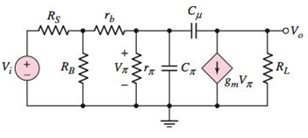
A common-emitter equivalent circuit is shown in Figure P7.50. (a) What isthe expression for the Miller capacitance? (b) Derive the expression for thevoltage gain A υ ( s ) = V o ( s ) / V i ( s ) in terms of the Miller capacitance andother circuit parameters. (c) What is the expression for the upper 3 dBfrequency? Figure P7.50
A common-emitter equivalent circuit is shown in Figure P7.50. (a) What isthe expression for the Miller capacitance? (b) Derive the expression for thevoltage gain A υ ( s ) = V o ( s ) / V i ( s ) in terms of the Miller capacitance andother circuit parameters. (c) What is the expression for the upper 3 dBfrequency? Figure P7.50
A common-emitter equivalent circuit is shown in Figure P7.50. (a) What isthe expression for the Miller capacitance? (b) Derive the expression for thevoltage gain
A
υ
(
s
)
=
V
o
(
s
)
/
V
i
(
s
)
in terms of the Miller capacitance andother circuit parameters. (c) What is the expression for the upper 3 dBfrequency?
Figure P7.50
(a)
Expert Solution
To determine
The expression for miller capacitance.
Answer to Problem 7.50P
The expression for miller capacitance is,
CM=Cμ(1+gmRL)
Explanation of Solution
Given:
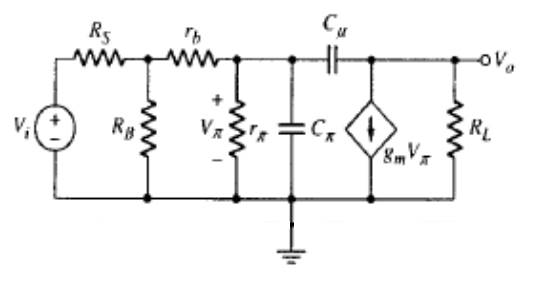
The given circuit is shown below.
Calculation:
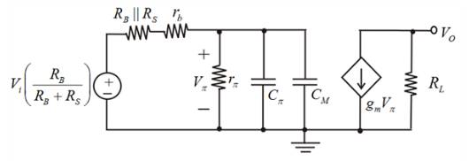
Draw the small signal equivalent circuit of figure including the equivalent miller capacitance
From figure, the thevenin voltage across the resistance RB is
VTH=Vi(RBRB+RS)
The equivalent thevenin resistance is,
RTH=RB∥RS
From above figure, the expression for output voltage is,
Vo=−gmVzRL
VoVπ=−gmRL
Av=−gmRL
Determine the expression for the Miller Capacitance.
Av=−gmRL
Determine the expression for the Miller Capacitance.
CM=Cμ(1+|Av|)
Substitute −gmRL for Av in the equation.
CM=Cμ(1+|−gmRL|)
=Cμ(1+gmRL)
Thus, the expression for miller capacitance is,
CM=Cμ(1+gmRL)
(b)
Expert Solution
To determine
The expression for voltage gain.
Answer to Problem 7.50P
The expression for voltage gain
Av(s)=(−βRLrπ+Req)(RBRB+RS)[11+s(rπ∥Req)Ci]
Explanation of Solution
Given:
The given circuit is shown below.
Calculation:
Draw the small signal equivalent circuit of figure including the equivalent miller capacitance
In figure, the capacitors Cx and CM are in parallel.
Ci=Cπ+CM
The value of total capacitive reactance is, 1sCi
Apply voltage division rule to write the expression for voltage Vπ
If the gain curve has a FWHM width of 1 GHz, what is the maximum numberof modes that can lase?
It is given as ?1 = ?3 = 50Ω and ?2 = 25Ω in the two-gate Π circuit given in the figure. According to this,a) Find the scattering matrix of the two-port circuit Π.b) Using the scattering matrix in a), determine the properties provided by the two-port circuit.
There exist several methods to perform AM demodulation, consider a requirement where we intend to design an AM receiver which is characterized by less distortion and high SNR.Identify which type of AM demodulation scheme is mentioned in the above statement and explain one such demodulation with appropriate sketch.Compare and contrast different AM modulation and demodulation schemes in various aspectsExplore one interesting application area involving Amplitude Modulation with explanation and neat sketch.
Need a deep-dive on the concept behind this application? Look no further. Learn more about this topic, electrical-engineering and related others by exploring similar questions and additional content below.


 Introductory Circuit Analysis (13th Edition)Electrical EngineeringISBN:9780133923605Author:Robert L. BoylestadPublisher:PEARSON
 Delmar's Standard Textbook Of ElectricityElectrical EngineeringISBN:9781337900348Author:Stephen L. HermanPublisher:Cengage Learning
 Programmable Logic ControllersElectrical EngineeringISBN:9780073373843Author:Frank D. PetruzellaPublisher:McGraw-Hill Education
 Fundamentals of Electric CircuitsElectrical EngineeringISBN:9780078028229Author:Charles K Alexander, Matthew SadikuPublisher:McGraw-Hill Education
 Electric Circuits. (11th Edition)Electrical EngineeringISBN:9780134746968Author:James W. Nilsson, Susan RiedelPublisher:PEARSON
 Engineering ElectromagneticsElectrical EngineeringISBN:9780078028151Author:Hayt, William H. (william Hart), Jr, BUCK, John A.Publisher:Mcgraw-hill Education,