
Videos
Consider the circuit shown in Figure P7.32. The transistor parameters are
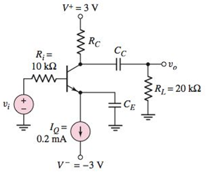
Figure P7.32
(a)
The value of
Answer to Problem 7.32P
The value of collector resistor,
Explanation of Solution
Given:
The given circuit is shown below.

Calculation:
From figure, the value of emitter current is,
The value of base current is,
Substitute
The value of collector current is,
Substitute
The value of emitter voltage is,
Substitute
The value of collector voltage is,
Substitute
The value of collector resistor is,
Substitute 3 V for
(b)
The mid band gain
Answer to Problem 7.32P
The value of mid-band gain
Explanation of Solution
Given:
The given circuit is shown below.

Calculation:
Draw the small signal equivalent circuit of figure to derive expression for mid band gain.
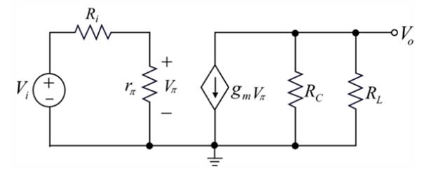
Apply voltage division rule to calculate the voltage across the base input resistor associated withthe input portion of the circuit.
Apply Kirchhoff's current law at output node in Figure 1
Substitute
The value of base input resistance.
Substitute
The value of transconductance is,
Substitute
The value of mid-band gain is,
Substitute
for
(c)
To derive: The expression for the corner frequencies associated with
Answer to Problem 7.32P
The expression for the corner frequency associated with
The expression for the corner frequency associated with
Explanation of Solution
Given:
The given circuit is shown below.

Calculation:
Derive the expression for the comer frequency associated with
Thus, the expression for the corner frequency associated with
Derive the expression for the comer frequency associated with
Thus, the expression for the corner frequency associated with
(d)
The value of
Answer to Problem 7.32P
The value of capacitance,
The value of capacitance,
Explanation of Solution
Given:
The given circuit is shown below.
Calculation:
Determine the value of capacitance,
Substitute
Thus, the value of capacitance,
Determine the value of capacitance,
Substitute
Thus, the value of capacitance,
Want to see more full solutions like this?
Chapter 7 Solutions
Microelectronics: Circuit Analysis and Design


- How many channels are available in the 2.4 GHz band? List all the channels. What is the channelbandwidth?arrow_forwardProblem1 A baseband signal with frequency components from near dc to 15 kHz frequency modulates a 200-kHz carrier, andthe frequency deviation is ±3 kHz. The signal is applied as the input to a cascade of two frequency triplers and onefrequency doubler. Determine the output (a) center frequency, (b) frequency deviation, and (c) deviation ratio (d) A VCO has an unmodulated carrier frequency of 100 MHz and sensitivity of −12 kHz#V. Determine thefrequency when the input signal is set at 5 V.arrow_forwarda) Sketch the spectrum of g(t)?b) Sketch the spectrum at point (a) of the conversion system?c) What should the parameter w0 be relative to wc?d) What should be the value of passband gain A?arrow_forward
- Briefly explain what it is Single Sideband Modulationarrow_forwardIf the frequency that is injected into an AM modulator is 100Mhz and it is combined with another injected signal of 10Khz, we can say that the combination is:arrow_forwardpls list the step by handwritinga) Sketch the spectrum of g(t)?b) Sketch the spectrum at point (a) of the conversion system?c) What should the parameter w0 be relative to wc?d) What should be the value of passband gain A?arrow_forward
- [Q1] A carrier signal (peak amplitude = 39V, frequency = 100MHz) is frequency modulated by the baseband signal (peak amplitude = 5V, bandwidth = 12.02kHz). The frequency deviation is 77.53kHz, and the load is 510. Determine (a) the load power, (b) the bandwidth of nsmitted signal. (consider only VnG)|> 0.1).arrow_forwardRegarding phase modulation (PM), an increase in the PM index, µ, results in an increase in the modulated signal’s bandwidth. (Explain) True Falsearrow_forwardWhen does maximum frequency deviation occur in an FM signal? -It occurs during the transition of the modulating signal to the opposite sign. -It occurs at the maximum amplitude point of the modulating signal. -It occurs during the maximum rate of change of the modulating signal. -It occurs at the mean point of the modulating signal.arrow_forward
- How do we get the smal signal model and why CL and Cb doesn’t short the resistance because of the high frequency?arrow_forwardExlapin any one method of suppression of unwanted sideband in detail. Neat answer sir!arrow_forwardQ1 ] A carrier signal ( peak amplitude = 39V , frequency = 100MHz ) frequency modulated by the baseband signal ( peak amplitude = 5V , bandwidth = 12.02kHz ) . The frequency deviation is 77.53kHz , and the load is 5112. Determine ( a ) the load power , ( b ) the bandwidth of the transmitted signal . ( consider only IJn ( $ ) > 0.1 ) .arrow_forward
 Introductory Circuit Analysis (13th Edition)Electrical EngineeringISBN:9780133923605Author:Robert L. BoylestadPublisher:PEARSON
 Delmar's Standard Textbook Of ElectricityElectrical EngineeringISBN:9781337900348Author:Stephen L. HermanPublisher:Cengage Learning
 Programmable Logic ControllersElectrical EngineeringISBN:9780073373843Author:Frank D. PetruzellaPublisher:McGraw-Hill Education
 Fundamentals of Electric CircuitsElectrical EngineeringISBN:9780078028229Author:Charles K Alexander, Matthew SadikuPublisher:McGraw-Hill Education
 Electric Circuits. (11th Edition)Electrical EngineeringISBN:9780134746968Author:James W. Nilsson, Susan RiedelPublisher:PEARSON
 Engineering ElectromagneticsElectrical EngineeringISBN:9780078028151Author:Hayt, William H. (william Hart), Jr, BUCK, John A.Publisher:Mcgraw-hill Education,