
Microelectronics: Circuit Analysis and Design
4th Edition
ISBN: 9780073380643
Author: Donald A. Neamen
Publisher: McGraw-Hill Companies, The
expand_more
expand_more
format_list_bulleted
Videos
Textbook Question
Chapter 7, Problem 7.15P
Consider the circuit shown in Figure P7.15. The transistor has parameters
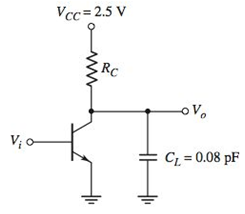
Figure P7.15
Expert Solution & Answer
Want to see the full answer?
Check out a sample textbook solution
Students have asked these similar questions
Bipolar junction transistors (BJTs) are considered “normally-off” devices, because their natural state with no signal applied to the base is no ........... between emitter and collector, like an open switch. * Your answer All field-effect transistors are unipolar rather than bipolar devices. That is, the main current through them is comprised either of ........... through an N-type semiconductor *
A modulating signal f(t) has a maximum
frequency of 18 kHz and peak
value of 3volt, this signal is encoded using
PCM.
1- Calculate the number of bits per sample if
the number of levels is 130
2- Calculate the SNRQ if the average power of
f(t) is 45 watt.
3- Calculate the minimum system bandwidth.
e 7:20
7.10 In Figure 7.25g, what is the voltage between the collector and 7.25(a) when , in the circuit of the Figure Earth if the current gain is 200?
Chapter 7 Solutions
Microelectronics: Circuit Analysis and Design
Ch. 7 - (a) For the circuit shown in Figure 7.2, the...Ch. 7 - The circuit shown in Figure 7.10 has parameters of...Ch. 7 - For the equivalent circuit shown in Figure 7.13,...Ch. 7 - The equivalent circuit in Figure 7.14 has circuit...Ch. 7 - The parameters in the circuit shown in Figure 7.15...Ch. 7 - For the circuit shown in Figure 7.2 1(a), the...Ch. 7 - Consider the circuit shown in Figure 7.22(a). The...Ch. 7 - For the emitterfollower circuit shown in Figure...Ch. 7 - The circuit shown in Figure 7.27(a) has parameters...Ch. 7 - Consider the common-base circuit shown in Figure...
Ch. 7 - The commonemitter circuit shown in Figure 7.34...Ch. 7 - A bipolar transistor has parameters o=120 ,...Ch. 7 - Prob. 7.9EPCh. 7 - For the circuit in Figure 7.41(a), the parameters...Ch. 7 - A bipolar transistor is biased at ICQ=120A and its...Ch. 7 - For the transistor described in Example 7.9 and...Ch. 7 - The parameters of a bipolar transistor are: o=150...Ch. 7 - The parameters of an nchannel MOSFET are...Ch. 7 - For the circuit in Figure 7.55, the transistor...Ch. 7 - An nchannel MOSFET has parameters Kn=0.4mA/V2 ,...Ch. 7 - An nchannel MOSFET has a unitygain bandwidth of...Ch. 7 - For a MOSFET, assume that gm=1.2mA/V . The basic...Ch. 7 - The transistor in the circuit in Figure 7.60 has...Ch. 7 - Consider the commonbase circuit in Figure 7.64....Ch. 7 - The cascode circuit in Figure 7.65 has parameters...Ch. 7 - Prob. 7.12TYUCh. 7 - For the circuit in Figure 7.72, the transistor...Ch. 7 - Describe the general frequency response of an...Ch. 7 - Describe the general characteristics of the...Ch. 7 - Describe what is meant by a system transfer...Ch. 7 - What is the criterion that defines a corner, or...Ch. 7 - Describe what is meant by the phase of the...Ch. 7 - Describe the time constant technique for...Ch. 7 - Describe the general frequency response of a...Ch. 7 - Sketch the expanded hybrid model of the BJT.Ch. 7 - Prob. 9RQCh. 7 - Prob. 10RQCh. 7 - Prob. 11RQCh. 7 - Sketch the expanded smallsignal equivalent circuit...Ch. 7 - Define the cutoff frequency for a MOSFET.Ch. 7 - Prob. 14RQCh. 7 - Why is there not a Miller effect in a commonbase...Ch. 7 - Describe the configuration of a cascode amplifier.Ch. 7 - Why is the bandwidth of a cascode amplifier...Ch. 7 - Why is the bandwidth of the emitterfollower...Ch. 7 - Prob. 7.1PCh. 7 - Prob. 7.2PCh. 7 - Consider the circuit in Figure P7.3. (a) Derive...Ch. 7 - Consider the circuit in Figure P7.4 with a signal...Ch. 7 - Consider the circuit shown in Figure P7.5. (a)...Ch. 7 - A voltage transfer function is given by...Ch. 7 - Sketch the Bode magnitude plots for the following...Ch. 7 - (a) Determine the transfer function corresponding...Ch. 7 - Consider the circuit shown in Figure 7.15 with...Ch. 7 - For the circuit shown in Figure P7.12, the...Ch. 7 - The circuit shown in Figure 7.10 has parameters...Ch. 7 - The transistor shown in Figure P7.14 has...Ch. 7 - Consider the circuit shown in Figure P7.15. The...Ch. 7 - The transistor in the circuit shown in Figure...Ch. 7 - For the common-emitter circuit in Figure P7.17,...Ch. 7 - The transistor in the circuit in Figure P7.20 has...Ch. 7 - For the circuit in Figure P7.21, the transistor...Ch. 7 - (a) For the circuit shown in Figure P7.22, write...Ch. 7 - Consider the circuit shown in Figure P7.23. (a)...Ch. 7 - The parameters of the transistor in the circuit in...Ch. 7 - A capacitor is placed in parallel with RL in the...Ch. 7 - The parameters of the transistor in the circuit in...Ch. 7 - Prob. D7.27PCh. 7 - The circuit in Figure P7.28 is a simple output...Ch. 7 - Reconsider the circuit in Figure P728. The...Ch. 7 - Consider the circuit shown in Figure P7.32. The...Ch. 7 - The commonemitter circuit in Figure P7.35 has an...Ch. 7 - Consider the commonbase circuit in Figure 7.33 in...Ch. 7 - Prob. 7.39PCh. 7 - The parameters of the transistor in the circuit in...Ch. 7 - In the commonsource amplifier in Figure 7.25(a) in...Ch. 7 - A bipolar transistor has fT=4GHz , o=120 , and...Ch. 7 - A highfrequency bipolar transistor is biased at...Ch. 7 - (a) The frequency fT of a bipolar transistor is...Ch. 7 - The circuit in Figure P7.48 is a hybrid ...Ch. 7 - Consider the circuit in Figure P7.49. Calculate...Ch. 7 - A common-emitter equivalent circuit is shown in...Ch. 7 - For the common-emitter circuit in Figure 7.41(a)...Ch. 7 - For the commonemitter circuit in Figure P7.52,...Ch. 7 - Consider the circuit in Figure P7.52. The resistor...Ch. 7 - The parameters of the circuit shown in Figure...Ch. 7 - The parameters of an nchannel MOSFET are kn=80A/V2...Ch. 7 - Find fT for a MOSFET biased at IDQ=120A and...Ch. 7 - Fill in the missing parameter values in the...Ch. 7 - (a) An nchannel MOSFET has an electron mobility of...Ch. 7 - A commonsource equivalent circuit is shown in...Ch. 7 - Prob. 7.60PCh. 7 - The parameters of an ideal nchannel MOSFET are...Ch. 7 - Figure P7.62 shows the highfrequency equivalent...Ch. 7 - For the FET circuit in Figure P7.63, the...Ch. 7 - The midband voltage gain of a commonsource MOSFET...Ch. 7 - Prob. 7.65PCh. 7 - Prob. 7.67PCh. 7 - The bias voltages of the circuit shown in Figure...Ch. 7 - For the PMOS commonsource circuit shown in Figure...Ch. 7 - In the commonbase circuit shown in Figure P7.70,...Ch. 7 - Repeat Problem 7.70 for the commonbase circuit in...Ch. 7 - In the commongate circuit in Figure P7.72, the...
Knowledge Booster


Learn more about
Need a deep-dive on the concept behind this application? Look no further. Learn more about this topic, electrical-engineering and related others by exploring similar questions and additional content below.Similar questions
- Q2. Consider the circuit shown in Figure P7.15. The transistor has parameters B = 120 and VA collector-emitter voltage is VCEO = 1.25 V. (a) Determine Rc, (b) find Ico, and (c) determine the maximum gain. = ∞. The circuit bandwidth is 800 MHz and the quiescent Vcc= 2.5 V RC CL = 0.08 pF Figure P7.15arrow_forwardThis problem is AC analysis problem. DC analysis is not needed to answer the question. A) If we assume that the peak voltage of Vbe must be less than 10 mV to avoid small signal violations determine the value of Rsig if Vi has a peak amplitude of 1 V and Is = 1mA. Hint: Don't forget r!! Answer: Rsig =. B) If you did the DC analysis on this problem and calculated Vc = 50 mV and Vs = -100 mV what is the maximum amplitude of the output voltage while the circuit stays in active mode. Answer: Vo,max =, When you "verify" a mode of operation you will need to calculate all three voltages (Vc, Ve, VE for BJTS and VG, Vs, Vp for MOSFETS) and show the correct two conditions are satisfied. Assume Capacitors acts like open circuits at DC and short circuits for AC. > Assume the following: 5V o Beta = 100 O VBE = 0.7 o V: (Thermal) = 26 mV o Vr (Threshold) = 2V O VA = - o For MOSFET saturation mode: assume: lp = K(VGs-Vr)? (Assume K = 10 mA/V²). 5kn C2 01 C1 Rsig 1kn 10k Vi IIs :C3 1mA -5Varrow_forwardDescribe the combined effect of the RC circuits for higher frequency response in a BJT & FETamplifier. the subject : Analogue Electronics IIarrow_forward
- In order to express the effect of the internal capacitors of BJT and the high frequency reception, the current gain expression depending on the frequency (Figure b) (hfe) is used in the case of collector emitter short circuit, voltage source connected at base end and emitter grounded (Figure la).. The catalog information of the 2N2222 transistor is given in Figure Ic. In the catalogue, when Ic=20 mA, it is seen as fT=250 MHz. a) Find the total capacitor effect for the case where gm> > wCμ. (Cpi) + (Cμ) = ?pFarrow_forward7.33 Figure P7.33 shows a discrete-circuit amplifier. The input signal vig is coupled to the gate through a very large capacitor (shown as infinite). The transistor source is connected to ground at signal frequencies via a very large capacitor (shown as infinite). The output voltage signal that develops at the drain is coupled to a load resistance via a very large capacitor (shown as infinite). All capacitors behave as short circuits for signals and as open circuits for de. (a) If the transistor has V, = 1 V, and k, = 4 mA/V', verify that the bias circuit establishes Ves = 1.5 V, I, =0.5 mA, and V, = +7.0 v. That is, assume these values, and %3D verify that they are consistent with the values of the circuit components and the device parameters. (b) Find g„, and r, if V, = 100 V. (c) Draw a complete small-signal equivalent circuit for the amplifier, assuming all capacitors behave as short circuits at signal frequencies. (d) Find R, V/vig, v,/Vg» and v,/vig- +15 V 10 MN 16 k2 Rie = 200…arrow_forwardConsider the common-base BJT amplifier in Figure 7. Assume that the following valuesremain constant during the operating conditions, B AC= 110 and VBE = 0.5V, Draw the ac equivalent circuit for the BJT amplifier circuit, and calculate the following ac values for the amplifier:i. R outii. R in(emitter) iii. Av iv. Ai v. Aparrow_forward
- Problem 7.133(a): For the circuit shown below, let R1 = 106 kN, Rsig = 69 N, and RL Rsig. Assume that %3D 13 kN. Find the value of the bias current I in mA that results in Rin the source provides a small signal vsie and that B = 100. H RL R1 Rsig Ria 8arrow_forwardExample 7 For the circuit shown, use R1=R2=47k2, RE=5.7k 22, RC=3.3k , RL=10k 2 and Vcc=12V, VBE=0.7V, B=100, IB=8.48uA 1-Draw the DC equivalent circuit. 2-Find the required parameter for the AC small signal model. 3-Draw the small signal model 4-Calculate the voltage gain. 5-Find the input impedance. 6-Find the output impedance. IB=8.84uA, IC=0.884mA, gm-35.36mA/V r=2.828KM. Usig Rin Gain=- 87.74, Rin=2.524k , Rout=3.3k Vcc R₁ R₂ Rc RE RL ww V Voarrow_forwardCoonsider the common emitter amplifier shown in figure below. Assume a β of 100, VBE = 0.7V, VT = 25mA and VA = 100V. Draw an equivalent DC model and determine the rπ, transconductance (gm) and ro. Draw an equaivalent AC model using the small-signal model Find an expression for vbe and vo in terms of the input voltagearrow_forward
- draw the following systems: 1- AM generation -Square law product. 2- PM generation- frequency modulator.arrow_forwardIn three-level PWM, the modulating process operates on each portion of the modulating function separately. The output peak value is still given by the depth of modulation, but the RMS value of the square wave is not Vin. Compute the THD for three-level PWM as a function of the depth of modulation (modulation index k).arrow_forwardGiven the MOSFET in Figure 6 has bran) = 200 mA at VGs = 4 V and V(Tn) = 2 V; i. Plot the transfer characteristic curve for the MOSFET. b) i. Determine the operating point Vasa, Ioa and Vosa for the circuit. ii. Calculate the value of the transconductance gm at the Q-point. iv. Determine the voltage gain and input impedance of the amplifier. 15 V 1 kn. Coe 1.5 M2. Cin 33 kn. Vn 30 ka Figure 6arrow_forward
arrow_back_ios
SEE MORE QUESTIONS
arrow_forward_ios
Recommended textbooks for you
 Introductory Circuit Analysis (13th Edition)Electrical EngineeringISBN:9780133923605Author:Robert L. BoylestadPublisher:PEARSON
 Delmar's Standard Textbook Of ElectricityElectrical EngineeringISBN:9781337900348Author:Stephen L. HermanPublisher:Cengage Learning
 Programmable Logic ControllersElectrical EngineeringISBN:9780073373843Author:Frank D. PetruzellaPublisher:McGraw-Hill Education
 Fundamentals of Electric CircuitsElectrical EngineeringISBN:9780078028229Author:Charles K Alexander, Matthew SadikuPublisher:McGraw-Hill Education
 Electric Circuits. (11th Edition)Electrical EngineeringISBN:9780134746968Author:James W. Nilsson, Susan RiedelPublisher:PEARSON
 Engineering ElectromagneticsElectrical EngineeringISBN:9780078028151Author:Hayt, William H. (william Hart), Jr, BUCK, John A.Publisher:Mcgraw-hill Education,
Introductory Circuit Analysis (13th Edition)
Electrical Engineering
ISBN:9780133923605
Author:Robert L. Boylestad
Publisher:PEARSON
Delmar's Standard Textbook Of Electricity
Electrical Engineering
ISBN:9781337900348
Author:Stephen L. Herman
Publisher:Cengage Learning
Programmable Logic Controllers
Electrical Engineering
ISBN:9780073373843
Author:Frank D. Petruzella
Publisher:McGraw-Hill Education
Fundamentals of Electric Circuits
Electrical Engineering
ISBN:9780078028229
Author:Charles K Alexander, Matthew Sadiku
Publisher:McGraw-Hill Education
Electric Circuits. (11th Edition)
Electrical Engineering
ISBN:9780134746968
Author:James W. Nilsson, Susan Riedel
Publisher:PEARSON
Engineering Electromagnetics
Electrical Engineering
ISBN:9780078028151
Author:Hayt, William H. (william Hart), Jr, BUCK, John A.
Publisher:Mcgraw-hill Education,
Diode Logic Gates - OR, NOR, AND, & NAND; Author: The Organic Chemistry Tutor;https://www.youtube.com/watch?v=9lqwSaIDm2g;License: Standard Youtube License