
Concept explainers
Videos
In the common−gate circuit in Figure P7.72, the transistor parameters are:
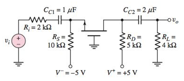
Figure P7.72
Want to see the full answer?
Check out a sample textbook solution
Chapter 7 Solutions
Microelectronics: Circuit Analysis and Design


- 7.65 In the circuit in Figure P7.65, the transistor parameters are: B = 120, VBE(on) = 0.7 V, VA = 100 V, C, = 1 pF, and fr = 600 MHz. (a) Deter- mine C, and the equivalent Miller capacitance Cy. State any approxima- tions or assumptions that you make. (b) Find the upper 3 dB frequency and the midband voltage gain. +5 V Rc-4 k2 R= 33 k2 Ccz =2 AF CCi =1 uF wwwHE Rg = 2 ka 35 k2 R2= 22 ka 4 ks2 ww ww wwarrow_forwardEXERCISE PROBLEM *Ex 7.13: The transistor in the circuit in Figure 7.60 has parameters B= 125, VBE(on) = 0.7 V, VA = 200 V, C = 24 pF, and C= 3 pF. (a) Calculate the Miller capacitance. (b) Determine the upper 3 dB frequency. (c) Determine the small-signal midband voltage gain. (Ans. (a) CM = 155 pF, (b) fH = 1.21 MHz, (c) A] = 37.3)arrow_forward7.65 In the circuit in Figure P7.65, the transistor parameters are: B = 120, VBE(on) = 0.7 V, VA = 100 V, C, = 1 pF, and fr = 600 MHz. (a) Deter- mine C, and the equivalent Miller capacitance CM. State any approxima- tions or assumptions that you make. (b) Find the upper 3 dB frequency and the midband voltage gain. Rc=D4 k2 R = 33 k2 C =1 uF Cc2 = 2 µF Rg = 2 k2 R = 5 ka R2 = 22 k2 Rg%3D 4 k2 Cg = 10 uF Figure P7.65 wwarrow_forward
- For an unmodulated carrier of 150 V and a modulated peak value of 230 V. What is the * percent modulation?arrow_forward(a) Design the circuit shown in Figure P7.18 such that Ipo = 0.8 mA, VDsQ = 3.2 V, Rin K, = 0.5 mA/V², VTN = 1.2 V, and A = 0. (b) What is the midband volt- age gain? (c) Determine the magnitude of the voltage gain at (i) f = 5 Hz, (ii) f = 14 Hz, and (iii) f = 25 Hz. (d) Sketch the Bode plot of the voltage gain magnitude and phase. 160 k2, and fr 16 Hz. The transistor parameters are ass VDD =9 V Rp R1 Rin 1 O vO Cc Rs = 0.5 k2 R2 Figure P7.18 ww wwarrow_forwardQuestion 2 (a) Briefly explain the advantage of the following Amplitude Modulation (AM) type and state ONE (1) application for each AM type: i. Double Sideband Full Carrier (DSBFC) ii. Double Sideband Suppressed Carrier (DSBSC) iii. Single Sideband (SSB). (b) The AM waveform for the modulated signal is illustrated in Figure 1. i. Calculate the percentage of modulation index, m. ii. State the type of the modulated signal. Justify the answer. iii. Write the equation for the modulated signal. iv. Calculate the percentage of power efficiency. 3V -1IV Figure 1arrow_forward
- 2. RLC Circuit a. Set up the circuit as shown in Figure 7.3. Apply 2Vpp voltage to Vin. L 0.01uF 100mH R Vin 100 Vo sine wave GND Figure 7.3 b. Calculate the resonant frequency fo of the circuit. c. Measure Vo when frequency of Function Generator is 1kHz, 2kHz, 4kHz, 6kHz, 8kHz, 10kHz and 20kHz.arrow_forwardQ2. For the scheme shown in Figure Q2, i. Draw the spectrum of the baseband signal (multiplexer output) for the multiplexer. ii. Determine the bandwidth of the baseband signal (multiplexer output) for the multiplexer. i. Determine the minimum transmission bandwidth of the multiplexer. Explain, briefly, the modification needed for the multiplexer in the figure to achieve this bandwidth. 4 kHz cos 10,000xt Basebund signal cos 24,000mt cos 2000mt cos 32,000nt Figure Q2arrow_forward2. Compare between TEmn and TMmn modes.arrow_forward
- The parameters of the circuit shown in Figure 1 are: B = 100, VBE = 0.7 V, VT = 26 mV, Cbc =12 pF, Cce= 15 pF and Cbe = 44 pF. Based on the circuit: i) Determine the midband voltage gain, A, = Vo. vi ii) Calculate the low cut-off frequencies caused by C1 and C2. iii) Calculate CE if the cut-off caused by this capacitor is 88 Hz. iv) Based on values in (ii) and (iii), what is the dominant low cut-off frequency? v) Determine the high cut-off frequency. +18V 3.3k2 C2=0.022µF C,=0.1µF V, 20k2 15k2 Vo 1k2 CE 6802 2.73V Vsarrow_forwardConsider the common source amplifier shown in the figure below. Assume that the transistorhas been biased in the saturation region. It has an ID = 1 mA, additionally k = 617 × 10−6 A/V2and Cgs = 1 pF. You may ignore channel length modulation and all other parasitic capacitors.Sketch the Bode plots for this amplifier.arrow_forwardHow it is generated Single Sideband Modulator Using Filter Methodarrow_forward
 Introductory Circuit Analysis (13th Edition)Electrical EngineeringISBN:9780133923605Author:Robert L. BoylestadPublisher:PEARSON
 Delmar's Standard Textbook Of ElectricityElectrical EngineeringISBN:9781337900348Author:Stephen L. HermanPublisher:Cengage Learning
 Programmable Logic ControllersElectrical EngineeringISBN:9780073373843Author:Frank D. PetruzellaPublisher:McGraw-Hill Education
 Fundamentals of Electric CircuitsElectrical EngineeringISBN:9780078028229Author:Charles K Alexander, Matthew SadikuPublisher:McGraw-Hill Education
 Electric Circuits. (11th Edition)Electrical EngineeringISBN:9780134746968Author:James W. Nilsson, Susan RiedelPublisher:PEARSON
 Engineering ElectromagneticsElectrical EngineeringISBN:9780078028151Author:Hayt, William H. (william Hart), Jr, BUCK, John A.Publisher:Mcgraw-hill Education,