
Videos
A BJT emitter follower is coupled to a load with an ideal transformer, as shown in Figure P8.35. The bias circuit is not shown. The transistor current gain is
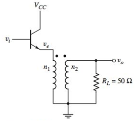
Figure P8.35
Want to see the full answer?
Check out a sample textbook solution
Chapter 8 Solutions
Microelectronics: Circuit Analysis and Design


- 4. The power dissipated in a resistance is equal to ..in non-sinusoidal input signal.arrow_forwardIn a full-bridge dc-dc converter using PWM bipolar voltage switching, analytically obtain the value of (V/V) which results in the maximum (peak-peak) ripple in the output current i,. Calculate this ripple in terms of Va, La, and farrow_forwardQUESTION 1 Design a high efficiency 3.3 V, 5A d.c.to d.c. power converter from a 4 to 5.5 Vdc source. The maximum allowable inductor current ripple and output voltage ripple are 0.1A and 20 mV, respectively. Assume a switching frequency of 20 kHz. a) Design a suitable converter power circuit using a MOSFET switch, showing all calculation of inductor and capacitor values and drawing a circuit diagram of the final design including component values. Indicate the peak inverse voltage and forward current rating of any diode required, and the maximum drain- source voltage of the MOSFET. b) On the Schematic diagram, draw the path of the current flow during the ON time and the OFF time. c) Describe the effect of changing the values of the inductor and the capacitor in the circuit. d) What is the effect of switching frequency in the circuit? e) Draw the schematic diagram of a circuit with the output voltage higher than the input voltage.arrow_forward
- 8.17c Copper extension leads are installed as shown in Figure 8.48b. For an output voltage of 7.947 mV and a reference junction temperature of 0⁰C, what is the temperature of the measuring junction?arrow_forwardDraw the AC equivalent circuit and find Zi, Zo, Av, Ai (ignore the effect of To). Show all the necessary derivations and label all the parameters properly.arrow_forward(a) Determine the input impedance of base if beta = 200(b) Determine the input impedance if Rc is changed to 680 ohm.(c) Draw the ac-equivalent circuit with beta = 150 (using T model).(d) Double all the resistances then, draw the ac-equivalent circuit for an ac current gain of300 (using Pi Model).arrow_forward
- Q.1) Consider a step down converter with a resistive load. It is supplied by a DC power source of magnitude Vs = 160 V. The switching period is 0.25 ms and the duty cycle k is first set to 0.5. The load is resistive with R=10 Ohms. The critical value of L and the critical value of C are equal to: a. 0.625mH and 0.392uF b. 0.625mH and 0.196uF c. 0.312mH and 0.196uF d. None of thesearrow_forwardQUESTION 4 In this voltage divider bias circuit, the input is at the base. Output is at the emitter with a high input resistance and low output resistance. The maximum voltage gain is 1 and the coupling capacitors must have a negligible reactance at the frequency of operation. (use to answer a and b) a. Derive the expression for the voltage gain, current gain, and power gain in terms of power delivered to the load, RL. b. Sketch both the DC and AC equivalent circuits. c. Derive the expression for ripple factor of Half Wave Rectification with a capacitor filter.arrow_forward2. A transformer-coupled class A amplifier drives an 8-ohm speaker through a 4:1 transformer. Using a power supply of Vcc = 36 V, the circuit delivers 3 W to the load. a. Calculate the following: i. Piecj across transformer primary. ii. Vuscd- ii. Vjac) at transformer primary. iv. The rms values of load and primary current. b. Draw the circuit diagram of a class A transformer-coupled amplifier using an npn transistor.arrow_forward
- 9. Design a biased-transistor circuit using VBB = Vcc= 10 V for a Q-point of Ic = 5 mA and VCE 4 V. Assume pc = 100. The design involves finding RB, RC, and the minimum power rating of the transistor. (The actual power rating should be greater.) Sketch the circuit.arrow_forwardQuestion 3: If the currents are in the same direction for a pair of parallel running wires, the currents on the wires are referred as Common Mode currents, ICM. On the other hand, if one of the currents is running in reverse direction (as they should normally do), the currents are referred as Differential Mode currents, IDM. It is essential in analog circuit design to keep track of differential and common mode currents. Referring to the following illustrations, assume that the separation between the wires, d, is 4 mm, the magnetic field observation point, S, is 20 mm away from the right wire, ICM- 5 mA, and IDM= 150 mA.arrow_forwardWithout changing the locations of the loads in the figure, a) Draw a suitable diagram to measure the active power drawn by the load Z2 ONLY using a W-m. b) According to your diagram, express the absolute method error in power measurement by defining the required magnitudes. (Give sufficient explanation). Z1 Z2 Z3 Z4arrow_forward
 Introductory Circuit Analysis (13th Edition)Electrical EngineeringISBN:9780133923605Author:Robert L. BoylestadPublisher:PEARSON
 Delmar's Standard Textbook Of ElectricityElectrical EngineeringISBN:9781337900348Author:Stephen L. HermanPublisher:Cengage Learning
 Programmable Logic ControllersElectrical EngineeringISBN:9780073373843Author:Frank D. PetruzellaPublisher:McGraw-Hill Education
 Fundamentals of Electric CircuitsElectrical EngineeringISBN:9780078028229Author:Charles K Alexander, Matthew SadikuPublisher:McGraw-Hill Education
 Electric Circuits. (11th Edition)Electrical EngineeringISBN:9780134746968Author:James W. Nilsson, Susan RiedelPublisher:PEARSON
 Engineering ElectromagneticsElectrical EngineeringISBN:9780078028151Author:Hayt, William H. (william Hart), Jr, BUCK, John A.Publisher:Mcgraw-hill Education,