
Concept explainers
(a)
Thevalue of the voltage
(a)
Answer to Problem 8.26P
The value of the voltage
Explanation of Solution
Calculation:
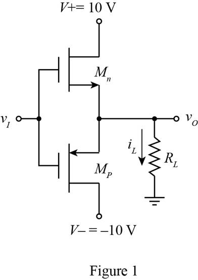
The given diagram is shown in Figure 1
The conversion from
The expression for the collector current is given by,
Substitute
The expression for the base emitter voltage of the NPN transistor for no input voltage is given by,
The expression for the base emitter voltage for the PNP transistor for zero input voltage is given by,
From the above equation and equation (1).
Substitute
The expression for the power dissipated in the transistor is given by,
Substitute
Conclusion:
Therefore, the value of the voltage
(b)
The value of the power dissipated in
(b)
Answer to Problem 8.26P
The value of
Explanation of Solution
Calculation:
The expression for the value of the load current is given by,
Substitute
The expression for the current through the PNP transistor is given by,
Substitute
The conversion from
The conversion from
The expression for the value of the base to emitter voltage of PNP transistor is given by,
Substitute
The expression to determine the value of the base emitter voltage of the NPN transistor is given by,
Substitute
The expression for the collector current of the NPN transistor is given by,
Substitute
The expression for the value of collector current of PNP transistor is given by,
Substitute
Apply KVL at the input terminals of the given figure.
Substitute
The expression for the power dissipated in the load is given by,
Substitute
The expression for the value of power dissipated in the transistor is given by,
Substitute
The expression for the power dissipated in the PNP transistor is given by,
Substitute
Conclusion:
Therefore, the value of
Want to see more full solutions like this?
Chapter 8 Solutions
Microelectronics: Circuit Analysis and Design


- Problem: Fx=(AB+CD+EF+G)' a. Draw its equivalent transistor circuit. b. Determine if the function has an Euler's path. please draw the equivalent Euler's path. C. Whether the circuit has a Euler's path or not, draw the stick diagram.arrow_forwardSince IDSS=8 mA, VGS(off) = -10V according to the circuit on the side, if the capacitor C2 is removed, what will be the Av gain value?arrow_forwardThe ac equivalent circuit for an amplifier is shown. Assume the capacitors have infinite value, RI = 100 kΩ, RG = 10 MΩ, RD = 560 kΩ, and R3 = 1.5 MΩ. Calculate the voltage gain for the amplifier if the MOSFETQ-point is (10 μA, 5 V). Assume Kn = 100 μA/V2 and λ = 0.02 V−1.arrow_forward
- In the circuit in the figure, VGSQ = 6.8 V, IDQ = 2.4 mA, VGS(Th) = 3.3 V, k = 0.4x10⁻³ A/V2, RD = 5.6 kΩ, RF = 2.2 MΩ and rd = 25 kΩ. Accordingly, when a RL = 0.1 kΩ load is connected to the output of the circuit, what will be the voltage gain of the circuit? NOTE: MOSFET output resistance must be taken into account in rd calculationsarrow_forwardThe transistor is specified to have Bf in the range of 7 to 35. The load resistance is Rc = 9 ohms. The dc supply voltage is Vcc = 180V and the input voltage to the base circuit is VB = 8V. If VCE (Sat) = 1,1 V and VBE (sat) = 1,6, determine: The value of RB that results in an ODF of 4 A. 0,7514 ohm B 0,5634 ohm C. 0,5081ohm D. 1 ohm The Power loss in the Transistor A. 35,07 W B. 44,30 W c. 40,04 W D. 23,65 Warrow_forwardIn the Mosfet circuit given below, R1+R2=50 kΩ, RD= 7.5 kΩ, VDD= 5V, VTP= -0.8 V, Kp= 0.2 mA/V2 is given. Calculate the ID current by determining the working region of the mosfet.arrow_forward
- Design a Single-Stage Common Emitter Class A Amplifier Specifications:Voltage Divider Bias Circuit Supply: Any value from 10Vdc to 24VdcLoad: 1kΩVoltage Gain: Any value from 80 to 400Lower Cutoff Frequency: 100 HzSinusoidal source (zero internal resistance): 50mVp-pTransistor: Si, β = 75 • Base-Collector capacitance = 8pF • Base-Emitter Capacitance = 25pF a) compute for the biasing resistances.b) determine the dc transistor terminal voltages and transistor currents.arrow_forwardThe topic is about BJT DC Analysis. Please show the correct and complete solution to this problem. Thank you!arrow_forwardNPN BJTs can be used as emitter followers. In the given circuit, the emitter follower is connected to a non-ideal voltage source (Vs) with a source resistance (Rs). Beta is 100, Vce,sat is 0V, and Vbe is 0.7V. 1. What is Vo if Vs = 3V and Rs = 5k ohms? 2. What is Vo if Vs = 3V and Rs = 0 ohms?arrow_forward
- How can you produce one sideband only? Suggest a method to obtain SSB.arrow_forwardGiven: Voltage Divider Bias Circuit Supply: 10Vdc to 24Vdc Load: 1000 ohms Voltage Gain: 80 to 400 Lower Cutt off Frequency: 100Hz Sinusoidal source (zero internal resistance): 50mVp-p Transistor: Si, beta=75 Base-Collector Capacitance= 8pF Base-Emitter Capacitance= 25pF Design a Single-stage Common Emitter Class A Amplifier and compute the following: a) dc load line b) hie c) midband gain d) Miller equivalent Capacitances e) upper cut off frequencyarrow_forwardAnswer as quickly as possible. I'll give upvote. Thank you. The circuit shown is a common source amplifier with a current mirror bias. It is given that the NMOS (M1) parameters are μoCox = 3mA/V2, VTH,n = 0.5V and λ = 0.02 and the PMOS (M2 and M3) parameters are μoCox = 1mA/V2 and VTH,p = −0.6V . The PMOS transistor M3 does not have channel length modulation while PMOS transistor M2 has λ = 0.02. It is also given that the dimensions of M2 and M3 have equal widths of 5µm and lengths of L2 = 3µm and L3 = 1.5µm, respectively. M1 has length of L1 = 1µm and width of W1 = 2µm. Find the gm and ro of transistor M1.arrow_forward
 Introductory Circuit Analysis (13th Edition)Electrical EngineeringISBN:9780133923605Author:Robert L. BoylestadPublisher:PEARSON
 Delmar's Standard Textbook Of ElectricityElectrical EngineeringISBN:9781337900348Author:Stephen L. HermanPublisher:Cengage Learning
 Programmable Logic ControllersElectrical EngineeringISBN:9780073373843Author:Frank D. PetruzellaPublisher:McGraw-Hill Education
 Fundamentals of Electric CircuitsElectrical EngineeringISBN:9780078028229Author:Charles K Alexander, Matthew SadikuPublisher:McGraw-Hill Education
 Electric Circuits. (11th Edition)Electrical EngineeringISBN:9780134746968Author:James W. Nilsson, Susan RiedelPublisher:PEARSON
 Engineering ElectromagneticsElectrical EngineeringISBN:9780078028151Author:Hayt, William H. (william Hart), Jr, BUCK, John A.Publisher:Mcgraw-hill Education,