
Microelectronics: Circuit Analysis and Design
4th Edition
ISBN: 9780073380643
Author: Donald A. Neamen
Publisher: McGraw-Hill Companies, The
expand_more
expand_more
format_list_bulleted
Videos
Textbook Question
Chapter 3, Problem 3.31P
For the circuit in Figure P3.31, the transistor parameters are
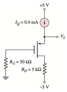
Figure P3.31
Expert Solution & Answer
Want to see the full answer?
Check out a sample textbook solution
Students have asked these similar questions
8 UTM Figure B.1 shows a diode circuit and its DC load line analysis. Based on the
SUT
information obtained
UT
UT
I kQ
+ VpQ-
3 UTM UTM
Vs
3
500 2
UTM & UM
TM &UTM UTM
UTM &UTM 5 UTM
Figure B.1
UTM & U UTM
VD (V)
0.72
UTM
i UTM
UTM
Which of the following is a type of Metal Oxide Semiconductor Field Effect Transistor:
O P channel JFET
O None of them
O N channel D- MOSFET
in
O N channel JFET
A simple diode rectifier has 'ripples in the output wave which makes it unsuitable as a DC source. To
overcome this one can use
of
a capacitor in series with a the load resistance.
stion
Select one:
O True
O False
Determine vo versus v₁ for the circuit shown in Figure 2. Assume that
the MOSFET operates in saturation and is characterized by the parameters K and VT.
Vs
R₁
www
Figure 2
wwww
RL
R₂
wwwww VO
Note: assuming the MOSFET works at normal saturation regime and
ips= (VDS -VT)²2
K
2
Chapter 3 Solutions
Microelectronics: Circuit Analysis and Design
Ch. 3 - An NMOS transistor with VTN=1V has a drain current...Ch. 3 - An PMOS device with VTP=1.2V has a drain current...Ch. 3 - (a) An nchannel enhancementmode MOSFET has a...Ch. 3 - The NMOS devices described in Exercise TYU 3.1...Ch. 3 - (a) A pchannel enhancementmode MOSFET has a...Ch. 3 - The PMOS devices described in Exercise TYU 3.3...Ch. 3 - The parameters of an NMOS enhancementmode device...Ch. 3 - An NMOS transistor has parameters VTNO=0.4V ,...Ch. 3 - Prob. 3.3EPCh. 3 - The transistor in Figure 3.26(a) has parameters...
Ch. 3 - For the transistor in the circuit in Figure 3.28,...Ch. 3 - Consider the circuit shown in Figure 3.30. The...Ch. 3 - Consider the circuit in Figure 3.30. Using the...Ch. 3 - (a) Consider the circuit shown in Figure 3.33. The...Ch. 3 - Consider the NMOS inverter shown in Figure 3.36...Ch. 3 - Consider the circuit shown in Figure 3.39 with...Ch. 3 - Consider the circuit in Figure 3.41. Assume the...Ch. 3 - Prob. 3.7TYUCh. 3 - Consider the circuit in Figure 3.43. The...Ch. 3 - For the circuit shown in Figure 3.36, use the...Ch. 3 - Consider the circuit shown in Figure 3.44. The...Ch. 3 - For the circuit shown in Figure 3.39, use the...Ch. 3 - For the MOS inverter circuit shown in Figure 3.45,...Ch. 3 - For the circuit in Figure 3.46, assume the circuit...Ch. 3 - The circuit shown in Figure 3.45 is biased at...Ch. 3 - The transistor in the circuit shown in Figure 3.48...Ch. 3 - In the circuit in Figure 3.46, let RD=25k and...Ch. 3 - For the circuit shown in Figure 3.49(a), assume...Ch. 3 - Prob. 3.15EPCh. 3 - Consider the constantcurrent source shown in...Ch. 3 - Consider the circuit in Figure 3.49(b). Assume...Ch. 3 - Consider the circuit shown in Figure 3.50. Assume...Ch. 3 - The transistor parameters for the circuit shown in...Ch. 3 - The transistor parameters for the circuit shown in...Ch. 3 - The parameters of an nchannel JFET are IDSS=12mA ,...Ch. 3 - The transistor in the circuit in Figure 3.62 has...Ch. 3 - For the pchannel transistor in the circuit in...Ch. 3 - Consider the circuit shown in Figure 3.66 with...Ch. 3 - The nchannel enhancementmode MESFET in the circuit...Ch. 3 - For the inverter circuit shown in Figure 3.68, the...Ch. 3 - Describe the basic structure and operation of a...Ch. 3 - Sketch the general currentvoltage characteristics...Ch. 3 - Describe what is meant by threshold voltage,...Ch. 3 - Describe the channel length modulation effect and...Ch. 3 - Describe a simple commonsource MOSFET circuit with...Ch. 3 - Prob. 6RQCh. 3 - In the dc analysis of some MOSFET circuits,...Ch. 3 - Prob. 8RQCh. 3 - Describe the currentvoltage relation of an...Ch. 3 - Describe the currentvoltage relation of an...Ch. 3 - Prob. 11RQCh. 3 - Describe how a MOSFET can be used to amplify a...Ch. 3 - Describe the basic operation of a junction FET.Ch. 3 - Prob. 14RQCh. 3 - (a) Calculate the drain current in an NMOS...Ch. 3 - The current in an NMOS transistor is 0.5 mA when...Ch. 3 - The transistor characteristics iD versus VDS for...Ch. 3 - For an nchannel depletionmode MOSFET, the...Ch. 3 - Verify the results of Example 3.4 with a PSpice...Ch. 3 - The threshold voltage of each transistor in Figure...Ch. 3 - The threshold voltage of each transistor in Figure...Ch. 3 - Consider an nchannel depletionmode MOSFET with...Ch. 3 - Determine the value of the process conduction...Ch. 3 - An nchannel enhancementmode MOSFET has parameters...Ch. 3 - Consider the NMOS circuit shown in Figure 3.36....Ch. 3 - An NMOS device has parameters VTN=0.8V , L=0.8m ,...Ch. 3 - Consider the NMOS circuit shown in Figure 3.39....Ch. 3 - A particular NMOS device has parameters VTN=0.6V ,...Ch. 3 - MOS transistors with very short channels do not...Ch. 3 - For a pchannel enhancementmode MOSFET, kp=50A/V2 ....Ch. 3 - For a pchannel enhancementmode MOSFET, the...Ch. 3 - The transistor characteristics iD versus SD for a...Ch. 3 - A pchannel depletionmode MOSFET has parameters...Ch. 3 - Calculate the drain current in a PMOS transistor...Ch. 3 - sDetermine the value of the process conduction...Ch. 3 - Enhancementmode NMOS and PMOS devices both have...Ch. 3 - For an NMOS enhancementmode transistor, the...Ch. 3 - The parameters of an nchannel enhancementmode...Ch. 3 - An enhancementmode NMOS transistor has parameters...Ch. 3 - An NMOS transistor has parameters VTO=0.75V ,...Ch. 3 - (a) A silicon dioxide gate insulator of an MOS...Ch. 3 - In a power MOS transistor, the maximum applied...Ch. 3 - In the circuit in Figure P3.26, the transistor...Ch. 3 - The transistor in the circuit in Figure P3.27 has...Ch. 3 - Prob. D3.28PCh. 3 - The transistor in the circuit in Figure P3.29 has...Ch. 3 - Consider the circuit in Figure P3.30. The...Ch. 3 - For the circuit in Figure P3.31, the transistor...Ch. 3 - Design a MOSFET circuit in the configuration shown...Ch. 3 - Consider the circuit shown in Figure P3.33. The...Ch. 3 - The transistor parameters for the transistor in...Ch. 3 - For the transistor in the circuit in Figure P3.35,...Ch. 3 - Design a MOSFET circuit with the configuration...Ch. 3 - The parameters of the transistors in Figures P3.37...Ch. 3 - For the circuit in Figure P3.38, the transistor...Ch. 3 - Prob. 3.39PCh. 3 - Prob. 3.40PCh. 3 - Design the circuit in Figure P3.41 so that...Ch. 3 - Prob. 3.42PCh. 3 - Prob. 3.43PCh. 3 - Prob. 3.44PCh. 3 - Prob. 3.45PCh. 3 - Prob. 3.46PCh. 3 - Prob. 3.47PCh. 3 - The transistors in the circuit in Figure 3.36 in...Ch. 3 - For the circuit in Figure 3.39 in the text, the...Ch. 3 - Prob. 3.50PCh. 3 - The transistor in the circuit in Figure P3.51 is...Ch. 3 - Prob. 3.52PCh. 3 - For the twoinput NMOS NOR logic gate in Figure...Ch. 3 - All transistors in the currentsource circuit shown...Ch. 3 - All transistors in the currentsource circuit shown...Ch. 3 - Consider the circuit shown in Figure 3.50 in the...Ch. 3 - The gate and source of an nchannel depletionmode...Ch. 3 - For an nchannel JFET, the parameters are IDSS=6mA...Ch. 3 - A pchannel JFET biased in the saturation region...Ch. 3 - Prob. 3.60PCh. 3 - Prob. 3.61PCh. 3 - The threshold voltage of a GaAs MESFET is...Ch. 3 - Prob. 3.63PCh. 3 - Prob. 3.64PCh. 3 - Prob. 3.65PCh. 3 - For the circuit in Figure P3.66, the transistor...Ch. 3 - Prob. 3.67PCh. 3 - Prob. 3.68PCh. 3 - For the circuit in Figure P3.69, the transistor...Ch. 3 - Prob. 3.70PCh. 3 - Prob. 3.71PCh. 3 - Prob. 3.72PCh. 3 - Using a computer simulation, verify the results of...Ch. 3 - Consider the PMOS circuit shown in Figure 3.30....Ch. 3 - Consider the circuit in Figure 3.39 with a...Ch. 3 - Prob. D3.79DPCh. 3 - Consider the multitransistor circuit in Figure...
Knowledge Booster


Learn more about
Need a deep-dive on the concept behind this application? Look no further. Learn more about this topic, electrical-engineering and related others by exploring similar questions and additional content below.Similar questions
- : For the given circuit, transistors and diodes are silicon where VD₁=VD2=0.7V and |VBE|=0.7V. Neglect base currents. a) Calculate VB1, VB2 which are base to ground DC voltages of Q1 and Q2, respectively b) Calculate the power generated by source c) Calculate the maximum power delivered to load and conversion efficiency Show your calculations step by step and fill the table. (Or you can draw the same table in your answer sheet). No ▷ D₁ D₂ 1K Q₁ +20V C HH RL=1002 a) VB₁[V] VB2 [V] b) PDC [W] c) PL[W] Efficiencyarrow_forwardFor the PN junction under sun light, the short circuit current amount is Isc. Please sketch the I-V curve of PN under the sun based on that under the dark condition above. Indicate Isc and Voc in your plot.arrow_forwardElectrical Engineering A uniformly doped silicon pnp bipolar transistor is to be designed with NĘ = 1019 cm³ and Nc = 1016 cm³. The metallurgical base width is 0.75 µm. Determine the minimum base doping so that the punch- through voltage is no less than 25 V.arrow_forward
- You have been given a Silicon-based BJT transistor with the leads labelled as shown in the figure: Plastic Body TO-92 1. Emitter 2. Base 3. Collector 123 Given that this transistor is either a PNP or NPN variant, create a step-by-step procedure for using a DMM with "diode check" feature to identify whether (a) it's an NPN or PNP (b) it's a PNP or NPN that has failed in some way (e.g. failed as open, or as a short)arrow_forward04:- Design a bias circuit for NPN silicon transistor having a nominal B-100 to be used in voltage divider circuit with Q-point of Ic 10 mA and VCE = 10 V. Use standard valued 5% resistors and draw a schematic diagram of your design. (10 points)arrow_forward3. Write down which transistor structure each curve characteristic belongs to in the figure. Ip -VGS -VGS +VGs (c) VGS (b) (a)arrow_forward
- For the circuit shown find: a. Power consumed in RL b. DC voltage of current source Ip dc. c. Q points of operation of the 2 transistors If it is not possible to calculate explain by laws. ID = 3 milliamperes. All semiconductors are silicon. Vcc 12 V BETA=100 ID Q1 D1 D2 Q2 100 Q D, 10 k2 VEE - 12 Varrow_forwardQ2/ For the Circuit shown below, Draw the DC load line and Determine the Q- point (take V BE = 0.7V B = 100) %3D Vcc = 30V RB 300K Rc = 2K IB B V CE IC E RE 1K IEarrow_forwardDerive the current equations for the circuit shown below, using the labels as shown.Note that rz here is a model of the parasitic imperfection of the Zener diode.a) IL = ?b) II = ?c) IZ = ?d) What impact does rz have on VL?arrow_forward
- ) For the following circuit, answer the following questions given that : Vz = 10 V, Iz= 25 mA, IzK= 1mA, Zz =72, PD(max) = 1 W at 50 °C. RA (N)=500 Determine the minimum and the maximum input voltages Vin (min), VIN (max) that can be regulated by the zener diode. Also, determine the line regulation. a) If a load resistor is connected, determine the minimum value of this load resistror R1(min) that can be used when VIN is set at 15 V. b) If the Zener derating factor is 2.8 mW/C, determine the maximum power the zener can dissipate at a temperature of 80 C. RA VIN VOUTarrow_forwardSet up a midpoint bias for a JFET with IDSS = 14 mA and VGS(off) = -10 V. Use a 24 V dc source as the supply voltage. Show the circuit and resistor values. Indicate the value of ID. Indicate the value of VGS. Indicate the value of VDS.arrow_forwardQ2 Design a voltage divider bias circuit for an npn silicon transistor having B = 100 to be used in a Common Emitter configuration. The quiescent point (Q point) is to be lc = 1 mA, VE = 5 V. The supply voltage (Vcc) is 15 V. Assume VĘ = 0.1Vc and BRĘ 2 10R2. (a)Find all the resistors values and draw the schematic diagram of this Common Emitter Amplifier with bypass capacitor Cę.arrow_forward
arrow_back_ios
SEE MORE QUESTIONS
arrow_forward_ios
Recommended textbooks for you
 Introductory Circuit Analysis (13th Edition)Electrical EngineeringISBN:9780133923605Author:Robert L. BoylestadPublisher:PEARSON
 Delmar's Standard Textbook Of ElectricityElectrical EngineeringISBN:9781337900348Author:Stephen L. HermanPublisher:Cengage Learning
 Programmable Logic ControllersElectrical EngineeringISBN:9780073373843Author:Frank D. PetruzellaPublisher:McGraw-Hill Education
 Fundamentals of Electric CircuitsElectrical EngineeringISBN:9780078028229Author:Charles K Alexander, Matthew SadikuPublisher:McGraw-Hill Education
 Electric Circuits. (11th Edition)Electrical EngineeringISBN:9780134746968Author:James W. Nilsson, Susan RiedelPublisher:PEARSON
 Engineering ElectromagneticsElectrical EngineeringISBN:9780078028151Author:Hayt, William H. (william Hart), Jr, BUCK, John A.Publisher:Mcgraw-hill Education,
Introductory Circuit Analysis (13th Edition)
Electrical Engineering
ISBN:9780133923605
Author:Robert L. Boylestad
Publisher:PEARSON
Delmar's Standard Textbook Of Electricity
Electrical Engineering
ISBN:9781337900348
Author:Stephen L. Herman
Publisher:Cengage Learning
Programmable Logic Controllers
Electrical Engineering
ISBN:9780073373843
Author:Frank D. Petruzella
Publisher:McGraw-Hill Education
Fundamentals of Electric Circuits
Electrical Engineering
ISBN:9780078028229
Author:Charles K Alexander, Matthew Sadiku
Publisher:McGraw-Hill Education
Electric Circuits. (11th Edition)
Electrical Engineering
ISBN:9780134746968
Author:James W. Nilsson, Susan Riedel
Publisher:PEARSON
Engineering Electromagnetics
Electrical Engineering
ISBN:9780078028151
Author:Hayt, William H. (william Hart), Jr, BUCK, John A.
Publisher:Mcgraw-hill Education,
How a MOSFET Works - with animation! | Intermediate Electronics; Author: CircuitBread;https://www.youtube.com/watch?v=Bfvyj88Hs_o;License: Standard Youtube License