
Microelectronics: Circuit Analysis and Design
4th Edition
ISBN: 9780073380643
Author: Donald A. Neamen
Publisher: McGraw-Hill Companies, The
expand_more
expand_more
format_list_bulleted
Videos
Textbook Question
Chapter 3, Problem 3.8TYU
Consider the circuit in Figure 3.43. The transistor parameters are
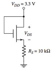
Figure 3.43 Circuit for Exercise TYU 3.8
Expert Solution & Answer
Want to see the full answer?
Check out a sample textbook solution
Students have asked these similar questions
A transistor current is given below. The Zener diode breakdown voltage is 5.3V as
shown. Take base to emitter voltage drop to be 0.6V. The value of the current gain
ß is .....
4.7kQ2
0.5mA ↓
5.3V
www
41
+
0.6-
www
22092
47092
04:- Design a bias circuit for NPN silicon transistor having a nominal B-100 to be used in voltage divider
circuit with Q-point of Ic 10 mA and VCE = 10 V. Use standard valued 5% resistors and draw a schematic
diagram of your design. (10 points)
A transistor has the CB input characteristics shown in Figure 3–11 (p. 106 ). If alpha = 0.95, find IC when VBE = 0.72 V and VCB = 10 V.
Chapter 3 Solutions
Microelectronics: Circuit Analysis and Design
Ch. 3 - An NMOS transistor with VTN=1V has a drain current...Ch. 3 - An PMOS device with VTP=1.2V has a drain current...Ch. 3 - (a) An nchannel enhancementmode MOSFET has a...Ch. 3 - The NMOS devices described in Exercise TYU 3.1...Ch. 3 - (a) A pchannel enhancementmode MOSFET has a...Ch. 3 - The PMOS devices described in Exercise TYU 3.3...Ch. 3 - The parameters of an NMOS enhancementmode device...Ch. 3 - An NMOS transistor has parameters VTNO=0.4V ,...Ch. 3 - Prob. 3.3EPCh. 3 - The transistor in Figure 3.26(a) has parameters...
Ch. 3 - For the transistor in the circuit in Figure 3.28,...Ch. 3 - Consider the circuit shown in Figure 3.30. The...Ch. 3 - Consider the circuit in Figure 3.30. Using the...Ch. 3 - (a) Consider the circuit shown in Figure 3.33. The...Ch. 3 - Consider the NMOS inverter shown in Figure 3.36...Ch. 3 - Consider the circuit shown in Figure 3.39 with...Ch. 3 - Consider the circuit in Figure 3.41. Assume the...Ch. 3 - Prob. 3.7TYUCh. 3 - Consider the circuit in Figure 3.43. The...Ch. 3 - For the circuit shown in Figure 3.36, use the...Ch. 3 - Consider the circuit shown in Figure 3.44. The...Ch. 3 - For the circuit shown in Figure 3.39, use the...Ch. 3 - For the MOS inverter circuit shown in Figure 3.45,...Ch. 3 - For the circuit in Figure 3.46, assume the circuit...Ch. 3 - The circuit shown in Figure 3.45 is biased at...Ch. 3 - The transistor in the circuit shown in Figure 3.48...Ch. 3 - In the circuit in Figure 3.46, let RD=25k and...Ch. 3 - For the circuit shown in Figure 3.49(a), assume...Ch. 3 - Prob. 3.15EPCh. 3 - Consider the constantcurrent source shown in...Ch. 3 - Consider the circuit in Figure 3.49(b). Assume...Ch. 3 - Consider the circuit shown in Figure 3.50. Assume...Ch. 3 - The transistor parameters for the circuit shown in...Ch. 3 - The transistor parameters for the circuit shown in...Ch. 3 - The parameters of an nchannel JFET are IDSS=12mA ,...Ch. 3 - The transistor in the circuit in Figure 3.62 has...Ch. 3 - For the pchannel transistor in the circuit in...Ch. 3 - Consider the circuit shown in Figure 3.66 with...Ch. 3 - The nchannel enhancementmode MESFET in the circuit...Ch. 3 - For the inverter circuit shown in Figure 3.68, the...Ch. 3 - Describe the basic structure and operation of a...Ch. 3 - Sketch the general currentvoltage characteristics...Ch. 3 - Describe what is meant by threshold voltage,...Ch. 3 - Describe the channel length modulation effect and...Ch. 3 - Describe a simple commonsource MOSFET circuit with...Ch. 3 - Prob. 6RQCh. 3 - In the dc analysis of some MOSFET circuits,...Ch. 3 - Prob. 8RQCh. 3 - Describe the currentvoltage relation of an...Ch. 3 - Describe the currentvoltage relation of an...Ch. 3 - Prob. 11RQCh. 3 - Describe how a MOSFET can be used to amplify a...Ch. 3 - Describe the basic operation of a junction FET.Ch. 3 - Prob. 14RQCh. 3 - (a) Calculate the drain current in an NMOS...Ch. 3 - The current in an NMOS transistor is 0.5 mA when...Ch. 3 - The transistor characteristics iD versus VDS for...Ch. 3 - For an nchannel depletionmode MOSFET, the...Ch. 3 - Verify the results of Example 3.4 with a PSpice...Ch. 3 - The threshold voltage of each transistor in Figure...Ch. 3 - The threshold voltage of each transistor in Figure...Ch. 3 - Consider an nchannel depletionmode MOSFET with...Ch. 3 - Determine the value of the process conduction...Ch. 3 - An nchannel enhancementmode MOSFET has parameters...Ch. 3 - Consider the NMOS circuit shown in Figure 3.36....Ch. 3 - An NMOS device has parameters VTN=0.8V , L=0.8m ,...Ch. 3 - Consider the NMOS circuit shown in Figure 3.39....Ch. 3 - A particular NMOS device has parameters VTN=0.6V ,...Ch. 3 - MOS transistors with very short channels do not...Ch. 3 - For a pchannel enhancementmode MOSFET, kp=50A/V2 ....Ch. 3 - For a pchannel enhancementmode MOSFET, the...Ch. 3 - The transistor characteristics iD versus SD for a...Ch. 3 - A pchannel depletionmode MOSFET has parameters...Ch. 3 - Calculate the drain current in a PMOS transistor...Ch. 3 - sDetermine the value of the process conduction...Ch. 3 - Enhancementmode NMOS and PMOS devices both have...Ch. 3 - For an NMOS enhancementmode transistor, the...Ch. 3 - The parameters of an nchannel enhancementmode...Ch. 3 - An enhancementmode NMOS transistor has parameters...Ch. 3 - An NMOS transistor has parameters VTO=0.75V ,...Ch. 3 - (a) A silicon dioxide gate insulator of an MOS...Ch. 3 - In a power MOS transistor, the maximum applied...Ch. 3 - In the circuit in Figure P3.26, the transistor...Ch. 3 - The transistor in the circuit in Figure P3.27 has...Ch. 3 - Prob. D3.28PCh. 3 - The transistor in the circuit in Figure P3.29 has...Ch. 3 - Consider the circuit in Figure P3.30. The...Ch. 3 - For the circuit in Figure P3.31, the transistor...Ch. 3 - Design a MOSFET circuit in the configuration shown...Ch. 3 - Consider the circuit shown in Figure P3.33. The...Ch. 3 - The transistor parameters for the transistor in...Ch. 3 - For the transistor in the circuit in Figure P3.35,...Ch. 3 - Design a MOSFET circuit with the configuration...Ch. 3 - The parameters of the transistors in Figures P3.37...Ch. 3 - For the circuit in Figure P3.38, the transistor...Ch. 3 - Prob. 3.39PCh. 3 - Prob. 3.40PCh. 3 - Design the circuit in Figure P3.41 so that...Ch. 3 - Prob. 3.42PCh. 3 - Prob. 3.43PCh. 3 - Prob. 3.44PCh. 3 - Prob. 3.45PCh. 3 - Prob. 3.46PCh. 3 - Prob. 3.47PCh. 3 - The transistors in the circuit in Figure 3.36 in...Ch. 3 - For the circuit in Figure 3.39 in the text, the...Ch. 3 - Prob. 3.50PCh. 3 - The transistor in the circuit in Figure P3.51 is...Ch. 3 - Prob. 3.52PCh. 3 - For the twoinput NMOS NOR logic gate in Figure...Ch. 3 - All transistors in the currentsource circuit shown...Ch. 3 - All transistors in the currentsource circuit shown...Ch. 3 - Consider the circuit shown in Figure 3.50 in the...Ch. 3 - The gate and source of an nchannel depletionmode...Ch. 3 - For an nchannel JFET, the parameters are IDSS=6mA...Ch. 3 - A pchannel JFET biased in the saturation region...Ch. 3 - Prob. 3.60PCh. 3 - Prob. 3.61PCh. 3 - The threshold voltage of a GaAs MESFET is...Ch. 3 - Prob. 3.63PCh. 3 - Prob. 3.64PCh. 3 - Prob. 3.65PCh. 3 - For the circuit in Figure P3.66, the transistor...Ch. 3 - Prob. 3.67PCh. 3 - Prob. 3.68PCh. 3 - For the circuit in Figure P3.69, the transistor...Ch. 3 - Prob. 3.70PCh. 3 - Prob. 3.71PCh. 3 - Prob. 3.72PCh. 3 - Using a computer simulation, verify the results of...Ch. 3 - Consider the PMOS circuit shown in Figure 3.30....Ch. 3 - Consider the circuit in Figure 3.39 with a...Ch. 3 - Prob. D3.79DPCh. 3 - Consider the multitransistor circuit in Figure...
Knowledge Booster


Learn more about
Need a deep-dive on the concept behind this application? Look no further. Learn more about this topic, electrical-engineering and related others by exploring similar questions and additional content below.Similar questions
- a) Figure B3 shows a cross section for a Metal Oxide Semiconductor Field Effect Transistor (MOSFET) in diagrammatic form. (i) (ii) Sketch the energy band diagram for the MOSFET along the line X-Y shown in Figure B3 when bias voltages are applied such that the silicon surface is inverted. Label all important features of your sketch and state any assumptions made. Sketch a box plot showing the charges present in the structure when the silicon surface is inverted. Indicate the source of all the charges and state whether they are positive or negative. Source n+ Metal Silicon Substrate - p X dioxide Drain n*arrow_forwardQ1) Answer True or False for the following: 1- Field-effect transistors are Bipolar devices. 2- A depletion MOSFET (D-MOSFET) can operate with a zero, positive, or negative gate-to source voltage. 3- The 4-layer diode is a thyristor that conducts when the voltage across its terminals exceeds the breakover potential. 4- The benefit of SCR Crowbar is power amplification. 5- Most op-amps require only a positive dc supply voltage.arrow_forward1. For a certain D-MOSFET, IDSS = 18 mA, and VGS = +10V. Vp =4V. a) Determine ID at VGS =+ 3V. b) Determine ID at VGS = -3V. %3Darrow_forward
- Determine vo versus v₁ for the circuit shown in Figure 2. Assume that the MOSFET operates in saturation and is characterized by the parameters K and VT. Vs R₁ www Figure 2 wwww RL R₂ wwwww VO Note: assuming the MOSFET works at normal saturation regime and ips= (VDS -VT)²2 K 2arrow_forward• In MOSFET, it is the foundation upon which the device will be constructed and is formed from a silicon base A. Substrate, B. Slab, C. Source, D. Base.arrow_forwardTransistorsFill in the blanks with the words below:amplify, bipolar transistor, current, device, embedded, field, field-effect transistor, fundamental,implemented, milestones, standardized, terminals, ubiquitous, vacuum tube, voltageA transistor is a semiconductor 1……….. used to amplify or switch electronic signals and electrical power. It iscomposed of semiconductor material usually with at least three 2 …………. for connection to an external circuit. A3. ………… or current applied to one pair of the transistor's terminals controls the current through another pair ofterminals. Because the controlled (output) power can be higher than the controlling (input) power, a transistor can4 …………… a signal. Today, some transistors are packaged individually, but many more are found 5 …………. inintegrated circuits.The transistor is the 6 …………. building block of modern electronic devices, and is 7. …………in modern electronicsystems. Julius Edgar Lilienfeld patented a 8 …………….. in 1926 but it was not…arrow_forward
- All field-effect transistors are unipolar rather than bipolar devices. That is, the main current through them is comprised either of through an N-type semiconductor * ..... .....arrow_forwardAn npn transistor has the CE input characteristics shown in Figure 3-19 (p. 115) and the CE output characteristics shown in Figure 3-20 (p. 115). (a) Find IB when VBE = 0.7 V and VCE = 20 V. (b) Find the beta of the transistor at VCE = 6.0 V and IB = 20uA (neglecting leakage). (c) Find bac for VCE = 6.0V and IB varying from 20 uA to 40 uA. (d) What is the approximate value of VCE,sat in Fig. 3-20?arrow_forwardYou have been given a Silicon-based BJT transistor with the leads labelled as shown in the figure: Plastic Body TO-92 1. Emitter 2. Base 3. Collector 123 Given that this transistor is either a PNP or NPN variant, create a step-by-step procedure for using a DMM with "diode check" feature to identify whether (a) it's an NPN or PNP (b) it's a PNP or NPN that has failed in some way (e.g. failed as open, or as a short)arrow_forward
- Figure 1 shows the typical output characteristics of MOSFET. Those characteristics show the difference curve of the drain current, Ip, as function of the drain- source voltage, VDs at a given gate-source voltage, VGs. In the Figure 1, it shows that the Ohmic region. What the meaning of the Ohmic region? Explain with necessary example any consequences that will happen for any condition of MOSFET. 360 10 V ev 7V 320 280 Ohmic region + 240 200 160 120 5.5 V- 80 40 2 3 Vos [V] Figure 1 lo [A]arrow_forwardQ1: for a silicon transistor in the figure below = 200 dc {What is the voltage between the collector and emitter VCE, drawing the load line and finding the Q pointarrow_forward8 UTM Figure B.1 shows a diode circuit and its DC load line analysis. Based on the SUT information obtained UT UT I kQ + VpQ- 3 UTM UTM Vs 3 500 2 UTM & UM TM &UTM UTM UTM &UTM 5 UTM Figure B.1 UTM & U UTM VD (V) 0.72 UTM i UTM UTMarrow_forward
arrow_back_ios
SEE MORE QUESTIONS
arrow_forward_ios
Recommended textbooks for you
 Introductory Circuit Analysis (13th Edition)Electrical EngineeringISBN:9780133923605Author:Robert L. BoylestadPublisher:PEARSON
 Delmar's Standard Textbook Of ElectricityElectrical EngineeringISBN:9781337900348Author:Stephen L. HermanPublisher:Cengage Learning
 Programmable Logic ControllersElectrical EngineeringISBN:9780073373843Author:Frank D. PetruzellaPublisher:McGraw-Hill Education
 Fundamentals of Electric CircuitsElectrical EngineeringISBN:9780078028229Author:Charles K Alexander, Matthew SadikuPublisher:McGraw-Hill Education
 Electric Circuits. (11th Edition)Electrical EngineeringISBN:9780134746968Author:James W. Nilsson, Susan RiedelPublisher:PEARSON
 Engineering ElectromagneticsElectrical EngineeringISBN:9780078028151Author:Hayt, William H. (william Hart), Jr, BUCK, John A.Publisher:Mcgraw-hill Education,
Introductory Circuit Analysis (13th Edition)
Electrical Engineering
ISBN:9780133923605
Author:Robert L. Boylestad
Publisher:PEARSON
Delmar's Standard Textbook Of Electricity
Electrical Engineering
ISBN:9781337900348
Author:Stephen L. Herman
Publisher:Cengage Learning
Programmable Logic Controllers
Electrical Engineering
ISBN:9780073373843
Author:Frank D. Petruzella
Publisher:McGraw-Hill Education
Fundamentals of Electric Circuits
Electrical Engineering
ISBN:9780078028229
Author:Charles K Alexander, Matthew Sadiku
Publisher:McGraw-Hill Education
Electric Circuits. (11th Edition)
Electrical Engineering
ISBN:9780134746968
Author:James W. Nilsson, Susan Riedel
Publisher:PEARSON
Engineering Electromagnetics
Electrical Engineering
ISBN:9780078028151
Author:Hayt, William H. (william Hart), Jr, BUCK, John A.
Publisher:Mcgraw-hill Education,
Diode Logic Gates - OR, NOR, AND, & NAND; Author: The Organic Chemistry Tutor;https://www.youtube.com/watch?v=9lqwSaIDm2g;License: Standard Youtube License