
Microelectronics: Circuit Analysis and Design
4th Edition
ISBN: 9780073380643
Author: Donald A. Neamen
Publisher: McGraw-Hill Companies, The
expand_more
expand_more
format_list_bulleted
Videos
Textbook Question
Chapter 3, Problem 3.41P
Design the circuit in Figure P3.41 so that
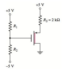
Figure P3.41
Expert Solution & Answer
Want to see the full answer?
Check out a sample textbook solution
Students have asked these similar questions
Design the following MOSFET circuit for it
to operate in saturation mode with 0.5 mA
drain current. Determine Rp and dc
voltage VĎ. Assume V₁ = 2 V and K = 0.1
mA/V² for this MOSFET.
10 V
RD
-VD
04:- Design a bias circuit for NPN silicon transistor having a nominal B-100 to be used in voltage divider
circuit with Q-point of Ic 10 mA and VCE = 10 V. Use standard valued 5% resistors and draw a schematic
diagram of your design. (10 points)
Problem5:
For the common base circurt shown in figure find I. and VCB. Assume transistor is
Silicon (a-0.98)
Ic
Rp= 1.5 ko
Rc= 1.2 kn
VEE = 8 V.
Vcc= 18 V
Chapter 3 Solutions
Microelectronics: Circuit Analysis and Design
Ch. 3 - An NMOS transistor with VTN=1V has a drain current...Ch. 3 - An PMOS device with VTP=1.2V has a drain current...Ch. 3 - (a) An nchannel enhancementmode MOSFET has a...Ch. 3 - The NMOS devices described in Exercise TYU 3.1...Ch. 3 - (a) A pchannel enhancementmode MOSFET has a...Ch. 3 - The PMOS devices described in Exercise TYU 3.3...Ch. 3 - The parameters of an NMOS enhancementmode device...Ch. 3 - An NMOS transistor has parameters VTNO=0.4V ,...Ch. 3 - Prob. 3.3EPCh. 3 - The transistor in Figure 3.26(a) has parameters...
Ch. 3 - For the transistor in the circuit in Figure 3.28,...Ch. 3 - Consider the circuit shown in Figure 3.30. The...Ch. 3 - Consider the circuit in Figure 3.30. Using the...Ch. 3 - (a) Consider the circuit shown in Figure 3.33. The...Ch. 3 - Consider the NMOS inverter shown in Figure 3.36...Ch. 3 - Consider the circuit shown in Figure 3.39 with...Ch. 3 - Consider the circuit in Figure 3.41. Assume the...Ch. 3 - Prob. 3.7TYUCh. 3 - Consider the circuit in Figure 3.43. The...Ch. 3 - For the circuit shown in Figure 3.36, use the...Ch. 3 - Consider the circuit shown in Figure 3.44. The...Ch. 3 - For the circuit shown in Figure 3.39, use the...Ch. 3 - For the MOS inverter circuit shown in Figure 3.45,...Ch. 3 - For the circuit in Figure 3.46, assume the circuit...Ch. 3 - The circuit shown in Figure 3.45 is biased at...Ch. 3 - The transistor in the circuit shown in Figure 3.48...Ch. 3 - In the circuit in Figure 3.46, let RD=25k and...Ch. 3 - For the circuit shown in Figure 3.49(a), assume...Ch. 3 - Prob. 3.15EPCh. 3 - Consider the constantcurrent source shown in...Ch. 3 - Consider the circuit in Figure 3.49(b). Assume...Ch. 3 - Consider the circuit shown in Figure 3.50. Assume...Ch. 3 - The transistor parameters for the circuit shown in...Ch. 3 - The transistor parameters for the circuit shown in...Ch. 3 - The parameters of an nchannel JFET are IDSS=12mA ,...Ch. 3 - The transistor in the circuit in Figure 3.62 has...Ch. 3 - For the pchannel transistor in the circuit in...Ch. 3 - Consider the circuit shown in Figure 3.66 with...Ch. 3 - The nchannel enhancementmode MESFET in the circuit...Ch. 3 - For the inverter circuit shown in Figure 3.68, the...Ch. 3 - Describe the basic structure and operation of a...Ch. 3 - Sketch the general currentvoltage characteristics...Ch. 3 - Describe what is meant by threshold voltage,...Ch. 3 - Describe the channel length modulation effect and...Ch. 3 - Describe a simple commonsource MOSFET circuit with...Ch. 3 - Prob. 6RQCh. 3 - In the dc analysis of some MOSFET circuits,...Ch. 3 - Prob. 8RQCh. 3 - Describe the currentvoltage relation of an...Ch. 3 - Describe the currentvoltage relation of an...Ch. 3 - Prob. 11RQCh. 3 - Describe how a MOSFET can be used to amplify a...Ch. 3 - Describe the basic operation of a junction FET.Ch. 3 - Prob. 14RQCh. 3 - (a) Calculate the drain current in an NMOS...Ch. 3 - The current in an NMOS transistor is 0.5 mA when...Ch. 3 - The transistor characteristics iD versus VDS for...Ch. 3 - For an nchannel depletionmode MOSFET, the...Ch. 3 - Verify the results of Example 3.4 with a PSpice...Ch. 3 - The threshold voltage of each transistor in Figure...Ch. 3 - The threshold voltage of each transistor in Figure...Ch. 3 - Consider an nchannel depletionmode MOSFET with...Ch. 3 - Determine the value of the process conduction...Ch. 3 - An nchannel enhancementmode MOSFET has parameters...Ch. 3 - Consider the NMOS circuit shown in Figure 3.36....Ch. 3 - An NMOS device has parameters VTN=0.8V , L=0.8m ,...Ch. 3 - Consider the NMOS circuit shown in Figure 3.39....Ch. 3 - A particular NMOS device has parameters VTN=0.6V ,...Ch. 3 - MOS transistors with very short channels do not...Ch. 3 - For a pchannel enhancementmode MOSFET, kp=50A/V2 ....Ch. 3 - For a pchannel enhancementmode MOSFET, the...Ch. 3 - The transistor characteristics iD versus SD for a...Ch. 3 - A pchannel depletionmode MOSFET has parameters...Ch. 3 - Calculate the drain current in a PMOS transistor...Ch. 3 - sDetermine the value of the process conduction...Ch. 3 - Enhancementmode NMOS and PMOS devices both have...Ch. 3 - For an NMOS enhancementmode transistor, the...Ch. 3 - The parameters of an nchannel enhancementmode...Ch. 3 - An enhancementmode NMOS transistor has parameters...Ch. 3 - An NMOS transistor has parameters VTO=0.75V ,...Ch. 3 - (a) A silicon dioxide gate insulator of an MOS...Ch. 3 - In a power MOS transistor, the maximum applied...Ch. 3 - In the circuit in Figure P3.26, the transistor...Ch. 3 - The transistor in the circuit in Figure P3.27 has...Ch. 3 - Prob. D3.28PCh. 3 - The transistor in the circuit in Figure P3.29 has...Ch. 3 - Consider the circuit in Figure P3.30. The...Ch. 3 - For the circuit in Figure P3.31, the transistor...Ch. 3 - Design a MOSFET circuit in the configuration shown...Ch. 3 - Consider the circuit shown in Figure P3.33. The...Ch. 3 - The transistor parameters for the transistor in...Ch. 3 - For the transistor in the circuit in Figure P3.35,...Ch. 3 - Design a MOSFET circuit with the configuration...Ch. 3 - The parameters of the transistors in Figures P3.37...Ch. 3 - For the circuit in Figure P3.38, the transistor...Ch. 3 - Prob. 3.39PCh. 3 - Prob. 3.40PCh. 3 - Design the circuit in Figure P3.41 so that...Ch. 3 - Prob. 3.42PCh. 3 - Prob. 3.43PCh. 3 - Prob. 3.44PCh. 3 - Prob. 3.45PCh. 3 - Prob. 3.46PCh. 3 - Prob. 3.47PCh. 3 - The transistors in the circuit in Figure 3.36 in...Ch. 3 - For the circuit in Figure 3.39 in the text, the...Ch. 3 - Prob. 3.50PCh. 3 - The transistor in the circuit in Figure P3.51 is...Ch. 3 - Prob. 3.52PCh. 3 - For the twoinput NMOS NOR logic gate in Figure...Ch. 3 - All transistors in the currentsource circuit shown...Ch. 3 - All transistors in the currentsource circuit shown...Ch. 3 - Consider the circuit shown in Figure 3.50 in the...Ch. 3 - The gate and source of an nchannel depletionmode...Ch. 3 - For an nchannel JFET, the parameters are IDSS=6mA...Ch. 3 - A pchannel JFET biased in the saturation region...Ch. 3 - Prob. 3.60PCh. 3 - Prob. 3.61PCh. 3 - The threshold voltage of a GaAs MESFET is...Ch. 3 - Prob. 3.63PCh. 3 - Prob. 3.64PCh. 3 - Prob. 3.65PCh. 3 - For the circuit in Figure P3.66, the transistor...Ch. 3 - Prob. 3.67PCh. 3 - Prob. 3.68PCh. 3 - For the circuit in Figure P3.69, the transistor...Ch. 3 - Prob. 3.70PCh. 3 - Prob. 3.71PCh. 3 - Prob. 3.72PCh. 3 - Using a computer simulation, verify the results of...Ch. 3 - Consider the PMOS circuit shown in Figure 3.30....Ch. 3 - Consider the circuit in Figure 3.39 with a...Ch. 3 - Prob. D3.79DPCh. 3 - Consider the multitransistor circuit in Figure...
Knowledge Booster


Learn more about
Need a deep-dive on the concept behind this application? Look no further. Learn more about this topic, electrical-engineering and related others by exploring similar questions and additional content below.Similar questions
- Identify the source, drain, gate, and bulk terminalsand find the current I in the transistorsAssume VTN = 0.70 Varrow_forwardA 10 V Zener diode is used to regulate the voltage across a variable loadresistor. The input voltage Vs varies between 13 and16 V. The loadcurrent (??) varies between 10 and 85 mA. The minimum Zener current is15 mA. Findi. The maximum value of Rsii. The maximum power dissipated by the Zener diode, using the value ofRs.arrow_forward2 What is the application of Diode? to protect the circuit from wrong DC voltage polarity connection. to convert the AC to AC. to resist the current. to charge and discharge the current 3 If you use PNP transistor and you want to switch ON the transistor, the base need positive curren negative current positive and negative current voltagearrow_forward
- A transistor current is given below. The Zener diode breakdown voltage is 5.3V as shown. Take base to emitter voltage drop to be 0.6V. The value of the current gain ß is ..... 4.7kQ2 0.5mA ↓ 5.3V www 41 + 0.6- www 22092 47092arrow_forwardA transistor has the CB input characteristics shown in Figure 3–11 (p. 106 ). If alpha = 0.95, find IC when VBE = 0.72 V and VCB = 10 V.arrow_forwardQ1: for a silicon transistor in the figure below = 200 dc {What is the voltage between the collector and emitter VCE, drawing the load line and finding the Q pointarrow_forward
- The junction between the base and collector of a transistor is called: O a. Collector Junction O b. Source Junction O c. Emitter Junction d. Base Junctionarrow_forwardAn npn transistor has the CE input characteristics shown in Figure 3-19 (p. 115) and the CE output characteristics shown in Figure 3-20 (p. 115). (a) Find IB when VBE = 0.7 V and VCE = 20 V. (b) Find the beta of the transistor at VCE = 6.0 V and IB = 20uA (neglecting leakage). (c) Find bac for VCE = 6.0V and IB varying from 20 uA to 40 uA. (d) What is the approximate value of VCE,sat in Fig. 3-20?arrow_forwardThe arrow on the symbol of MOSFET indicates O a. that it is a N-channel MOSFET O b. that it is a P-channel MOSFET Oc. the direction of electrons O d. the direction of conventional current flowarrow_forward
- An NPN silicon transistor having a nominal ß of 100 is to be used in a CE configuration with Vcc= 15 V. The Q point is to be Ic = 4mA and VcE = 12V . Now design the circuit diagram.arrow_forward• In MOSFET, it is the foundation upon which the device will be constructed and is formed from a silicon base A. Substrate, B. Slab, C. Source, D. Base.arrow_forwardQ2: A transistor dissipates 50W in an ambient temperature of 60°C, the thermal resistances are 0-0.5 °CW¹, 8ca-4 °CW'. Determine the junction temperature without a heat sink. Determine the thermal resistance of the heat sink to avoid the junction temperature exceeding 180°C. 3arrow_forward
arrow_back_ios
SEE MORE QUESTIONS
arrow_forward_ios
Recommended textbooks for you
 Introductory Circuit Analysis (13th Edition)Electrical EngineeringISBN:9780133923605Author:Robert L. BoylestadPublisher:PEARSON
 Delmar's Standard Textbook Of ElectricityElectrical EngineeringISBN:9781337900348Author:Stephen L. HermanPublisher:Cengage Learning
 Programmable Logic ControllersElectrical EngineeringISBN:9780073373843Author:Frank D. PetruzellaPublisher:McGraw-Hill Education
 Fundamentals of Electric CircuitsElectrical EngineeringISBN:9780078028229Author:Charles K Alexander, Matthew SadikuPublisher:McGraw-Hill Education
 Electric Circuits. (11th Edition)Electrical EngineeringISBN:9780134746968Author:James W. Nilsson, Susan RiedelPublisher:PEARSON
 Engineering ElectromagneticsElectrical EngineeringISBN:9780078028151Author:Hayt, William H. (william Hart), Jr, BUCK, John A.Publisher:Mcgraw-hill Education,
Introductory Circuit Analysis (13th Edition)
Electrical Engineering
ISBN:9780133923605
Author:Robert L. Boylestad
Publisher:PEARSON
Delmar's Standard Textbook Of Electricity
Electrical Engineering
ISBN:9781337900348
Author:Stephen L. Herman
Publisher:Cengage Learning
Programmable Logic Controllers
Electrical Engineering
ISBN:9780073373843
Author:Frank D. Petruzella
Publisher:McGraw-Hill Education
Fundamentals of Electric Circuits
Electrical Engineering
ISBN:9780078028229
Author:Charles K Alexander, Matthew Sadiku
Publisher:McGraw-Hill Education
Electric Circuits. (11th Edition)
Electrical Engineering
ISBN:9780134746968
Author:James W. Nilsson, Susan Riedel
Publisher:PEARSON
Engineering Electromagnetics
Electrical Engineering
ISBN:9780078028151
Author:Hayt, William H. (william Hart), Jr, BUCK, John A.
Publisher:Mcgraw-hill Education,
Diode Logic Gates - OR, NOR, AND, & NAND; Author: The Organic Chemistry Tutor;https://www.youtube.com/watch?v=9lqwSaIDm2g;License: Standard Youtube License