
Microelectronics: Circuit Analysis and Design
4th Edition
ISBN: 9780073380643
Author: Donald A. Neamen
Publisher: McGraw-Hill Companies, The
expand_more
expand_more
format_list_bulleted
Videos
Textbook Question
Chapter 3, Problem 3.38P
For the circuit in Figure P3.38, the transistor parameters are
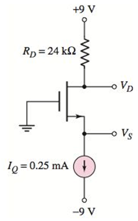
Figure P3.38
Expert Solution & Answer
Want to see the full answer?
Check out a sample textbook solution
Students have asked these similar questions
Q-3. Find the drain-source voltage, Vos, for the E- MOSFET circuit given below. The device parameters are: Ioss = 4
mA and Vm = 2 V.
+15V
Rp-
2k
4M
R1
+
Vps
2M
R2
Given the PMOSFET circuit below with VDD = 5 V, and
characteristics k = 75 μA/V², Vth = 0.75V and R = 10000; solve
for the drain voltage and drain current
VDD
R
VD = ?
ww
iD = ?
Determine vo versus v₁ for the circuit shown in Figure 2. Assume that
the MOSFET operates in saturation and is characterized by the parameters K and VT.
Vs
R₁
www
Figure 2
wwww
RL
R₂
wwwww VO
Note: assuming the MOSFET works at normal saturation regime and
ips= (VDS -VT)²2
K
2
Chapter 3 Solutions
Microelectronics: Circuit Analysis and Design
Ch. 3 - An NMOS transistor with VTN=1V has a drain current...Ch. 3 - An PMOS device with VTP=1.2V has a drain current...Ch. 3 - (a) An nchannel enhancementmode MOSFET has a...Ch. 3 - The NMOS devices described in Exercise TYU 3.1...Ch. 3 - (a) A pchannel enhancementmode MOSFET has a...Ch. 3 - The PMOS devices described in Exercise TYU 3.3...Ch. 3 - The parameters of an NMOS enhancementmode device...Ch. 3 - An NMOS transistor has parameters VTNO=0.4V ,...Ch. 3 - Prob. 3.3EPCh. 3 - The transistor in Figure 3.26(a) has parameters...
Ch. 3 - For the transistor in the circuit in Figure 3.28,...Ch. 3 - Consider the circuit shown in Figure 3.30. The...Ch. 3 - Consider the circuit in Figure 3.30. Using the...Ch. 3 - (a) Consider the circuit shown in Figure 3.33. The...Ch. 3 - Consider the NMOS inverter shown in Figure 3.36...Ch. 3 - Consider the circuit shown in Figure 3.39 with...Ch. 3 - Consider the circuit in Figure 3.41. Assume the...Ch. 3 - Prob. 3.7TYUCh. 3 - Consider the circuit in Figure 3.43. The...Ch. 3 - For the circuit shown in Figure 3.36, use the...Ch. 3 - Consider the circuit shown in Figure 3.44. The...Ch. 3 - For the circuit shown in Figure 3.39, use the...Ch. 3 - For the MOS inverter circuit shown in Figure 3.45,...Ch. 3 - For the circuit in Figure 3.46, assume the circuit...Ch. 3 - The circuit shown in Figure 3.45 is biased at...Ch. 3 - The transistor in the circuit shown in Figure 3.48...Ch. 3 - In the circuit in Figure 3.46, let RD=25k and...Ch. 3 - For the circuit shown in Figure 3.49(a), assume...Ch. 3 - Prob. 3.15EPCh. 3 - Consider the constantcurrent source shown in...Ch. 3 - Consider the circuit in Figure 3.49(b). Assume...Ch. 3 - Consider the circuit shown in Figure 3.50. Assume...Ch. 3 - The transistor parameters for the circuit shown in...Ch. 3 - The transistor parameters for the circuit shown in...Ch. 3 - The parameters of an nchannel JFET are IDSS=12mA ,...Ch. 3 - The transistor in the circuit in Figure 3.62 has...Ch. 3 - For the pchannel transistor in the circuit in...Ch. 3 - Consider the circuit shown in Figure 3.66 with...Ch. 3 - The nchannel enhancementmode MESFET in the circuit...Ch. 3 - For the inverter circuit shown in Figure 3.68, the...Ch. 3 - Describe the basic structure and operation of a...Ch. 3 - Sketch the general currentvoltage characteristics...Ch. 3 - Describe what is meant by threshold voltage,...Ch. 3 - Describe the channel length modulation effect and...Ch. 3 - Describe a simple commonsource MOSFET circuit with...Ch. 3 - Prob. 6RQCh. 3 - In the dc analysis of some MOSFET circuits,...Ch. 3 - Prob. 8RQCh. 3 - Describe the currentvoltage relation of an...Ch. 3 - Describe the currentvoltage relation of an...Ch. 3 - Prob. 11RQCh. 3 - Describe how a MOSFET can be used to amplify a...Ch. 3 - Describe the basic operation of a junction FET.Ch. 3 - Prob. 14RQCh. 3 - (a) Calculate the drain current in an NMOS...Ch. 3 - The current in an NMOS transistor is 0.5 mA when...Ch. 3 - The transistor characteristics iD versus VDS for...Ch. 3 - For an nchannel depletionmode MOSFET, the...Ch. 3 - Verify the results of Example 3.4 with a PSpice...Ch. 3 - The threshold voltage of each transistor in Figure...Ch. 3 - The threshold voltage of each transistor in Figure...Ch. 3 - Consider an nchannel depletionmode MOSFET with...Ch. 3 - Determine the value of the process conduction...Ch. 3 - An nchannel enhancementmode MOSFET has parameters...Ch. 3 - Consider the NMOS circuit shown in Figure 3.36....Ch. 3 - An NMOS device has parameters VTN=0.8V , L=0.8m ,...Ch. 3 - Consider the NMOS circuit shown in Figure 3.39....Ch. 3 - A particular NMOS device has parameters VTN=0.6V ,...Ch. 3 - MOS transistors with very short channels do not...Ch. 3 - For a pchannel enhancementmode MOSFET, kp=50A/V2 ....Ch. 3 - For a pchannel enhancementmode MOSFET, the...Ch. 3 - The transistor characteristics iD versus SD for a...Ch. 3 - A pchannel depletionmode MOSFET has parameters...Ch. 3 - Calculate the drain current in a PMOS transistor...Ch. 3 - sDetermine the value of the process conduction...Ch. 3 - Enhancementmode NMOS and PMOS devices both have...Ch. 3 - For an NMOS enhancementmode transistor, the...Ch. 3 - The parameters of an nchannel enhancementmode...Ch. 3 - An enhancementmode NMOS transistor has parameters...Ch. 3 - An NMOS transistor has parameters VTO=0.75V ,...Ch. 3 - (a) A silicon dioxide gate insulator of an MOS...Ch. 3 - In a power MOS transistor, the maximum applied...Ch. 3 - In the circuit in Figure P3.26, the transistor...Ch. 3 - The transistor in the circuit in Figure P3.27 has...Ch. 3 - Prob. D3.28PCh. 3 - The transistor in the circuit in Figure P3.29 has...Ch. 3 - Consider the circuit in Figure P3.30. The...Ch. 3 - For the circuit in Figure P3.31, the transistor...Ch. 3 - Design a MOSFET circuit in the configuration shown...Ch. 3 - Consider the circuit shown in Figure P3.33. The...Ch. 3 - The transistor parameters for the transistor in...Ch. 3 - For the transistor in the circuit in Figure P3.35,...Ch. 3 - Design a MOSFET circuit with the configuration...Ch. 3 - The parameters of the transistors in Figures P3.37...Ch. 3 - For the circuit in Figure P3.38, the transistor...Ch. 3 - Prob. 3.39PCh. 3 - Prob. 3.40PCh. 3 - Design the circuit in Figure P3.41 so that...Ch. 3 - Prob. 3.42PCh. 3 - Prob. 3.43PCh. 3 - Prob. 3.44PCh. 3 - Prob. 3.45PCh. 3 - Prob. 3.46PCh. 3 - Prob. 3.47PCh. 3 - The transistors in the circuit in Figure 3.36 in...Ch. 3 - For the circuit in Figure 3.39 in the text, the...Ch. 3 - Prob. 3.50PCh. 3 - The transistor in the circuit in Figure P3.51 is...Ch. 3 - Prob. 3.52PCh. 3 - For the twoinput NMOS NOR logic gate in Figure...Ch. 3 - All transistors in the currentsource circuit shown...Ch. 3 - All transistors in the currentsource circuit shown...Ch. 3 - Consider the circuit shown in Figure 3.50 in the...Ch. 3 - The gate and source of an nchannel depletionmode...Ch. 3 - For an nchannel JFET, the parameters are IDSS=6mA...Ch. 3 - A pchannel JFET biased in the saturation region...Ch. 3 - Prob. 3.60PCh. 3 - Prob. 3.61PCh. 3 - The threshold voltage of a GaAs MESFET is...Ch. 3 - Prob. 3.63PCh. 3 - Prob. 3.64PCh. 3 - Prob. 3.65PCh. 3 - For the circuit in Figure P3.66, the transistor...Ch. 3 - Prob. 3.67PCh. 3 - Prob. 3.68PCh. 3 - For the circuit in Figure P3.69, the transistor...Ch. 3 - Prob. 3.70PCh. 3 - Prob. 3.71PCh. 3 - Prob. 3.72PCh. 3 - Using a computer simulation, verify the results of...Ch. 3 - Consider the PMOS circuit shown in Figure 3.30....Ch. 3 - Consider the circuit in Figure 3.39 with a...Ch. 3 - Prob. D3.79DPCh. 3 - Consider the multitransistor circuit in Figure...
Knowledge Booster


Learn more about
Need a deep-dive on the concept behind this application? Look no further. Learn more about this topic, electrical-engineering and related others by exploring similar questions and additional content below.Similar questions
- For the circuit in Figure below, what is Ic3? Assume all transistors are identical. IREF 1 Q5 R1 IREF2 O IE of Q2 O 2 IREF1 O IE of Q1 Vh1 Q6 Q1 03 07 8 Vn2 04 IREF2 R2arrow_forwardQ2 Design a voltage divider bias circuit for an npn silicon transistor having B %D 100 to be used in a Common Emitter configuration. The quiescent point = 1 mA, VCE = 5 V. The supply voltage (Vcc) is 15 V. (Q point) is to be l. Assume VĘ = 0.1Vcc and BRĘ 2 10R2. (a)Find all the resistors values and draw the schematic diagram of this Common Emitter Amplifier with bypass capacitor CE.arrow_forward6. Current mirror All MOSFETS in the circuit below have V, = 1 V and k, = 2 mA/V² (A = 0). Q1 and Q2 form a current mirror that supplics drain current to Q3. Calculate Ip and Vout: + 5 V 8 k Q3 o Vout Q1 Q2 -5 varrow_forward
- Determine Rout for the Common Source E-MOSFET circuit in the figure. Assume this particular MOSFET has minimum values of ID(on) = 200 mA at VGS = 4 V and VGS(th) = 2 V. %3D %3D VDD +24 V Rp 200 N R 100 kN R2 15 kNarrow_forwardGiven the PMOSFET circuit below with VDD = 5 V, and characteristics k = 75 µA/V², Vth = 0.75V and R = 10000; solve for the drain voltage and drain current Note: Take caution in the units used for k and R. Your answer must be accurate to 1 decimal place. VDD VD =? iD = ?arrow_forwardCalculate the resistance value, Rs needed for a p-channel JFET transistor circuit if you know that IDss = 25 mA, VGSS (off) = 15V, and VGs = 5V. %3Darrow_forward
- Given the PMOSFET circuit below with VDD = 5 V, and characteristics k = 25 µA/V², Vth = 0.75V and R = 100; solve for the drain voltage and drain current Note: Take caution in the units used for k and R. Your answer must be accurate to 1 decimal place. iD VDD Parameter UD R UD = ? iD = ? Value μA mVarrow_forwardConsider an nMOS with tox=9 nm, µn=500cm²/Vs, Vt=0.7V, and W/L=10. Find the drain currents for the following cases: i. Ves=5 and VDs=5V ii. Ves=5 V and VDs=1Varrow_forwardFor the circuit shown in Figure Vec= 22 V, Re= 5.6Kr Nc %3D R8- 330k2, B= 80 Rc Rg %3D Find the solution to Vi everything that comes 1_value of Zo .....ohm . NOTE: 1.2ks 3 The value of re is . . h is When the output is taken from the Emitter terminal of 0.47ks3 the transistor as shown in Figure. CE 2 The value of Zi is 4 The value of Ai is . wwarrow_forward
- In the circuit in the figure below the reading of the voltmeter is [V] V. Determine the amount of drain current (in mA). Assume this particular MOSFET has minimum values of loon) = 200 mA at Vas 4 V and Vash)=2 V. vl RG ww 10 MO Vpe 1 Rp 4.7 karrow_forwardGiven the PMOSFET circuit below with VDD = 5 V, and characteristics k = 25 μA/V2, Vth = 0.75V and R = 100, solve for the drain voltage and drain currentarrow_forward. For the circuit shown in figure. For the eircait stown in Figure If Vec 35 V, IE 3.22 mA VE = () Vec. Vec 300k RE The value of Beta is .. ...* O 53.93 O 57.39 O 55.93 54.93 O 51.39 O 56.39 The value of Vc is . . Volt.." O 21.24 O 29.24 O 24.27 O 23.25 O 25.24 O 27.24 O O O O O O Oarrow_forward
arrow_back_ios
SEE MORE QUESTIONS
arrow_forward_ios
Recommended textbooks for you
 Introductory Circuit Analysis (13th Edition)Electrical EngineeringISBN:9780133923605Author:Robert L. BoylestadPublisher:PEARSON
 Delmar's Standard Textbook Of ElectricityElectrical EngineeringISBN:9781337900348Author:Stephen L. HermanPublisher:Cengage Learning
 Programmable Logic ControllersElectrical EngineeringISBN:9780073373843Author:Frank D. PetruzellaPublisher:McGraw-Hill Education
 Fundamentals of Electric CircuitsElectrical EngineeringISBN:9780078028229Author:Charles K Alexander, Matthew SadikuPublisher:McGraw-Hill Education
 Electric Circuits. (11th Edition)Electrical EngineeringISBN:9780134746968Author:James W. Nilsson, Susan RiedelPublisher:PEARSON
 Engineering ElectromagneticsElectrical EngineeringISBN:9780078028151Author:Hayt, William H. (william Hart), Jr, BUCK, John A.Publisher:Mcgraw-hill Education,
Introductory Circuit Analysis (13th Edition)
Electrical Engineering
ISBN:9780133923605
Author:Robert L. Boylestad
Publisher:PEARSON
Delmar's Standard Textbook Of Electricity
Electrical Engineering
ISBN:9781337900348
Author:Stephen L. Herman
Publisher:Cengage Learning
Programmable Logic Controllers
Electrical Engineering
ISBN:9780073373843
Author:Frank D. Petruzella
Publisher:McGraw-Hill Education
Fundamentals of Electric Circuits
Electrical Engineering
ISBN:9780078028229
Author:Charles K Alexander, Matthew Sadiku
Publisher:McGraw-Hill Education
Electric Circuits. (11th Edition)
Electrical Engineering
ISBN:9780134746968
Author:James W. Nilsson, Susan Riedel
Publisher:PEARSON
Engineering Electromagnetics
Electrical Engineering
ISBN:9780078028151
Author:Hayt, William H. (william Hart), Jr, BUCK, John A.
Publisher:Mcgraw-hill Education,
How a MOSFET Works - with animation! | Intermediate Electronics; Author: CircuitBread;https://www.youtube.com/watch?v=Bfvyj88Hs_o;License: Standard Youtube License