
Microelectronics: Circuit Analysis and Design
4th Edition
ISBN: 9780073380643
Author: Donald A. Neamen
Publisher: McGraw-Hill Companies, The
expand_more
expand_more
format_list_bulleted
Videos
Textbook Question
Chapter 2, Problem 2.19P
Consider the circuit shown in Figure P2.19. The Zener diode voltage is
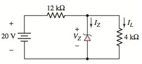
Figure P2.19
Expert Solution & Answer
Want to see the full answer?
Check out a sample textbook solution
Students have asked these similar questions
Figure Q2 (b) shows the Zener diode circuit . Given PzM (maximum power) =
40mW. Assume the Zener diode is ideal. Determine:
(c)
(1)
V.
(ii)
Iz
(iii) Pz
R=10002
16V
Iz
Vz
9V
3kn
Figure Q2 (b)
Determine Q-point for the diodes in the circuit given below using the ideal diode model where, R1 = 12.2 kΩ, R2 = 16 kΩ, and R3 = 14 kΩ. (Note: Label the diodes from left to right.)
Consider the circuit shown in Figure 2. The cut-in voltage of each diode is . Let and
assume both diodes are conducting. Determine if this is a valid assumption and
explain your answer. And calculate the values of IR, ID, Ip2, and V..
Rj =1.7 kQ
ww
VB =1 V
D1
Dz
R2D
4 kQ
Figure 2
Chapter 2 Solutions
Microelectronics: Circuit Analysis and Design
Ch. 2 - Repeat Example 2.1 if the input voltage is...Ch. 2 - Consider the bridge circuit shown in Figure 2.6(a)...Ch. 2 - Assume the input signal to a rectifier circuit has...Ch. 2 - The input voltage to the halfwave rectifier in...Ch. 2 - Consider the circuit in Figure 2.4. The input...Ch. 2 - The circuit in Figure 2.5(a) is used to rectify a...Ch. 2 - The secondary transformer voltage of the rectifier...Ch. 2 - Determine the fraction (percent) of the cycle that...Ch. 2 - The Zener diode regulator circuit shown in Figure...Ch. 2 - Repeat Example 2.6 for rz=4 . Assume all other...
Ch. 2 - Consider the circuit shown in Figure 2.19. Let...Ch. 2 - Suppose the currentlimiting resistor in Example...Ch. 2 - Suppose the power supply voltage in the circuit...Ch. 2 - Design a parallelbased clipper that will yield the...Ch. 2 - Sketch the steadystate output voltage for the...Ch. 2 - Consider the circuit in Figure 2.23(a). Let R1=5k...Ch. 2 - Determine the steadystate output voltage O for the...Ch. 2 - Design a parallelbased clipper circuit that will...Ch. 2 - Consider the circuit shown in Figure 2.38, in...Ch. 2 - Consider the circuit shown in Figure 2.39. The...Ch. 2 - Repeat Example 2.11 for the case when R1=8k ,...Ch. 2 - The cutin voltage of each diode in the circuit...Ch. 2 - Prob. 2.12TYUCh. 2 - Consider the OR logic circuit shown in Figure...Ch. 2 - Consider the AND logic circuit shown in Figure...Ch. 2 - (a) Photons with an energy of hv=2eV are incident...Ch. 2 - Determine the value of resistance R required to...Ch. 2 - What characteristic of a diode is used in the...Ch. 2 - Prob. 2RQCh. 2 - Describe a simple fullwave diode rectifier circuit...Ch. 2 - Prob. 4RQCh. 2 - Prob. 5RQCh. 2 - Describe a simple Zener diode voltage reference...Ch. 2 - What effect does the Zener diode resistance have...Ch. 2 - What are the general characteristics of diode...Ch. 2 - Describe a simple diode clipper circuit that...Ch. 2 - Prob. 10RQCh. 2 - What one circuit element, besides a diode, is...Ch. 2 - Prob. 12RQCh. 2 - Describe a diode OR logic circuit. Compare a logic...Ch. 2 - Describe a diode AND logic circuit. Compare a...Ch. 2 - Describe a simple circuit that can be used to turn...Ch. 2 - Consider the circuit shown in Figure P2.1. Let...Ch. 2 - For the circuit shown in Figure P2.1, show that...Ch. 2 - A halfwave rectifier such as shown in Figure...Ch. 2 - Consider the battery charging circuit shown in...Ch. 2 - Figure P2.5 shows a simple fullwave battery...Ch. 2 - The fullwave rectifier circuit shown in Figure...Ch. 2 - The input signal voltage to the fullwave rectifier...Ch. 2 - The output resistance of the fullwave rectifier in...Ch. 2 - Repeat Problem 2.8 for the halfwave rectifier in...Ch. 2 - Consider the halfwave rectifier circuit shown in...Ch. 2 - The parameters of the halfwave rectifier circuit...Ch. 2 - The fullwave rectifier circuit shown in Figure...Ch. 2 - Consider the fullwave rectifier circuit in Figure...Ch. 2 - The circuit in Figure P2.14 is a complementary...Ch. 2 - Prob. 2.15PCh. 2 - A fullwave rectifier is to be designed using the...Ch. 2 - Prob. 2.17PCh. 2 - (a) Sketch o versus time for the circuit in Figure...Ch. 2 - Consider the circuit shown in Figure P2.19. The...Ch. 2 - Consider the Zener diode circuit shown in Figure...Ch. 2 - Consider the Zener diode circuit shown in Figure...Ch. 2 - In the voltage regulator circuit in Figure P2.21,...Ch. 2 - A Zener diode is connected in a voltage regulator...Ch. 2 - Consider the Zener diode circuit in Figure 2.19 in...Ch. 2 - Design a voltage regulator circuit such as shown...Ch. 2 - The percent regulation of the Zener diode...Ch. 2 - A voltage regulator is to have a nominal output...Ch. 2 - Consider the circuit in Figure P2.28. Let V=0 ....Ch. 2 - The secondary voltage in the circuit in Figure...Ch. 2 - The parameters in the circuit shown in Figure...Ch. 2 - Consider the circuit in Figure P2.31. Let V=0 (a)...Ch. 2 - Prob. 2.32PCh. 2 - Each diode cutin voltage is 0.7 V for the circuits...Ch. 2 - The diode in the circuit of Figure P2.34(a) has...Ch. 2 - Consider the circuits shown in Figure P2.35. Each...Ch. 2 - Plot O for each circuit in Figure P2.36 for the...Ch. 2 - Consider the parallel clipper circuit in Figure...Ch. 2 - A car’s radio may be subjected to voltage spikes...Ch. 2 - Sketch the steadystate output voltage O versus...Ch. 2 - Prob. D2.40PCh. 2 - Design a diode clamper to generate a steadystate...Ch. 2 - For the circuit in Figure P2.39(b), let V=0 and...Ch. 2 - Repeat Problem 2.42 for the circuit in Figure...Ch. 2 - The diodes in the circuit in Figure P2.44 have...Ch. 2 - In the circuit in Figure P2.45 the diodes have the...Ch. 2 - The diodes in the circuit in Figure P2.46 have the...Ch. 2 - Consider the circuit shown in Figure P2.47. Assume...Ch. 2 - The diode cutin voltage for each diode in the...Ch. 2 - Consider the circuit in Figure P2.49. Each diode...Ch. 2 - Assume V=0.7V for each diode in the circuit in...Ch. 2 - The cutin voltage of each diode in the circuit...Ch. 2 - Let V=0.7V for each diode in the circuit in Figure...Ch. 2 - For the circuit shown in Figure P2.54, let V=0.7V...Ch. 2 - Assume each diode cutin voltage is V=0.7V for the...Ch. 2 - If V=0.7V for the diode in the circuit in Figure...Ch. 2 - Let V=0.7V for the diode in the circuit in Figure...Ch. 2 - Each diode cutin voltage in the circuit in Figure...Ch. 2 - Let V=0.7V for each diode in the circuit shown in...Ch. 2 - Consider the circuit in Figure P2.61. The output...Ch. 2 - Consider the circuit in Figure P2.62. The output...Ch. 2 - Prob. 2.63PCh. 2 - Consider the circuit shown in Figure P2.64. The...Ch. 2 - The lightemitting diode in the circuit shown in...Ch. 2 - The parameters of D1 and D2 in the circuit shown...Ch. 2 - If the resistor in Example 2.12 is R=2 and the...Ch. 2 - Consider the photodiode circuit shown in Figure...Ch. 2 - Consider the fullwave bridge rectifier circuit....Ch. 2 - Design a simple dc voltage source using a...Ch. 2 - A clipper is to be designed such that O=2.5V for...Ch. 2 - Design a circuit to provide the voltage transfer...
Knowledge Booster


Learn more about
Need a deep-dive on the concept behind this application? Look no further. Learn more about this topic, electrical-engineering and related others by exploring similar questions and additional content below.Similar questions
- How is a solid-state diode tested? Explain.arrow_forwardFigure Q2(a) shows the characteristic curve of a Zener diode. Analyse the characteristic curve to identify the approximate minimum Zener current Izk(min) and the approximate Zener voltage, Vz at IZK. -10 -9 -8 -7 -6 -5 -2 -1 Vz (V) + 1 3 4 6 7 8 Iz (mA) Figure Q2(a) Analyse the circuit in Figure Q2(b) to identify the minimum input voltage required to keep the diode in Zener region based on the values of the minimum Zener current and the approximated Zener voltage found in Question 2(a). R 1k2 VIN Figure Q2(b)arrow_forwardPower supply circuit is delivering 0.5 A and an average voltage 20 V to the load as shown in the circuit below. The ripple voltage of the half wave rectifier is 0.5 V and the diode is represented using constant voltage model. The smoothing capacitor value is equal to 220V rmsh soHz} VL-DC =20V 0.01 F 0.02 F 0.0167 F None of the abovearrow_forward
- Determine Q-point for the diodes in the circuit given below using the constant voltage drop model with Von = 0.65 V, where R₁ = 15.2 k2, R2 = 24 k2, and R3 = 22 k. (Note: Label the diodes from left to right.) Q +2 V -10 V D1: ( D2: D3: ( R₁ www www K Küün 즈 mA, mA, mA, OV и ऽऽऽ R₂ www R3 -5 Varrow_forwardFor the circuit shown in the Figure, if the diodes are silicon diodes with Vp(on)=0.7 V, and VIN=50 sin wt V, V1 =6 V and V2 = 16 V, then the value of VouTP-p) is: R, D VaN Vout v1事 2章 Oa. 25.4 V Ob. 27.4 V Oc. 29.4 V Od. 23.4 Varrow_forwardQ2:- Find the level of Vo for each circuit shown in the Figure below. Also, determine the status of each diode; if it is forward or reverses biasing. Assume all diodes are silicone with 0.7v drop. +5 V +15 V -10 V (12 Marks) R DI +5 VoK D +5 VoK DI -5 VoH -5 Vo4 D2 D2 D2 +5 VoH D3 +5 Vo4 D3 -10 VoK D4 V. -5 Vo K (a) (b)arrow_forward
- The four diodes used in a bridge rectifier circuit have forward resistances which may be considered constant at 1 ohm and infinite reverse resistance. The alternating supply voltage is 220 V r.m.s. and load resistance is 580 ohm. Calculate (i) mean load current and (ii) power dissipated in each diode.arrow_forwardDraw the input waveform and output waveform for the circuit given below with proper values marked in the figure. Assume D1 as germanium and D2 as silicon diodes. Input Vpp%3D20V, V1=3 V and V2=10 V. R D2 D1 Vin Vout V1 V2 Maximum voltage of output waveform Minimum voltage of output waveform Psarrow_forwardConsider the Zener diode circuit shown in Figure. The Zener Breakdown Voltage (Vz) is 5.6 V at Iz= 0.1mA. Zener resistance is r,= 10 0. What is Vo without load (RL= ∞) ? R= 0.5 kQ Vo Vps= 10 Varrow_forward
- 0:- Consider the circuit in Figure a) What type of circuit is this? b) Find and Sketch the voltage waveform across RL, assume the diodes are practical. c) If 100uf capacitor parallel with the resistor, calculate the ripple is connected factor I O o Darrow_forwardDraw the input waveform and output waveform for the circuit given below with proper values marked in the figure. Assume D1 as silicon and D2 as germanium diodes. Input Vpp=20V. V1=5 V and V2=9 V. R www D1 Vin Vout v1 V2 Maximum voltage of output waveform Minimum voltage of output waveformarrow_forward2. Figure A.1 shows I-V characteristics of two diodes, namely A and B. Diode A has higher dynamic resistance than diode B. UTM &UT ID 4 5UTM 3TM UTM UTM &UTM 5 UTM & UTM UTM 3 UTM 03 TM 6 UT 0.68 (a) UTM VD Figure A.1 State one possible reason why the diodes have different knee voltage values. UTM OM & UTM 3 UTM & TM (b) Based on Figure A.1, identify the knee voltage of UTM" TM 5 UTde BE UTMarrow_forward
arrow_back_ios
SEE MORE QUESTIONS
arrow_forward_ios
Recommended textbooks for you

Three-Phase Half-Wave Rectifier Operation; Author: katkimshow;https://www.youtube.com/watch?v=Uhbr6tbMB9A;License: Standard Youtube License