
Videos
Consider the circuit shown in Figure P2.47. Assume each diode cut−in voltage is
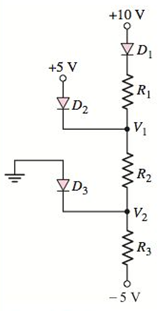
Figure P2.47
(a)
The values of
Answer to Problem 2.47P
The required values are,
Explanation of Solution
Given:
Diode’s cut-in voltage =
Calculation:
Assume all diode are conducting.
Draw the circuit diagram with node voltages and cut-in voltages.
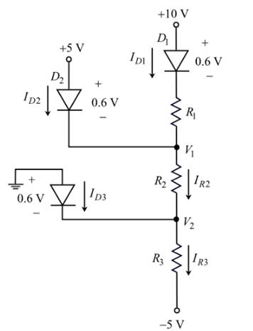
Figure 1
From Figure 1, the voltage at node
The voltage at node
Write the expression for current following through diode
Substitute
Therefore, the value of the resistor,
Apply Kirchhoff’s current law at node
Substitute
Calculate the value of resistor
Substitute
Therefore, the value of the resistor
Apply Kirchhoff’s current law at node
Substitute
Calculate the value of resistor
Substitute
Therefore, the value of the resistor,
Conclusion:
Therefore, the required values are
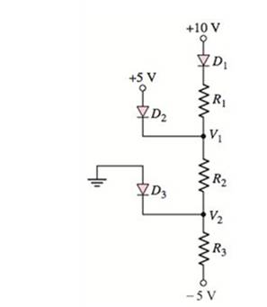
(b)
To find: The values of
Answer to Problem 2.47P
The required values are,
Explanation of Solution
Given:
Diode’s cut-in volt- age is
Calculation:
Assume at diodes are conducting.
From Figure 1, the voltage at node
The voltage at node
Calculate the current,
Substitute
Therefore, the current following through diode
Calculate the current following through resistor
Substitute
Apply Kirchhoff’s current law at node
Substitute
Therefore, the current following diode
Calculate the current following through resistor,
Substitute
Apply Kirchhoff’s current law at node
Substitute
Therefore, the current following diode
Conclusion:
Therefore, the required values are
(c)
To find: The values of
Answer to Problem 2.47P
The require values are
Explanation of Solution
Given:
Diode’s cut-in volt- age is

Calculation:
Assume diode
Draw the current diagram with node voltage and cut-in voltages.
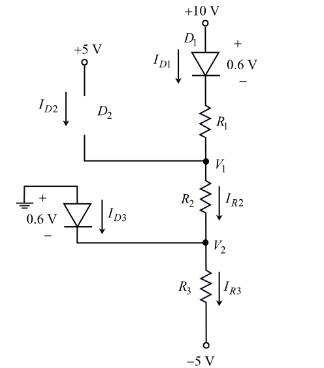
Figure 2
In Figure 2, the Diode
That is,
Therefore, the current following through diode
From Figure 2, the voltage at node
Apply Kirchhoff’s current law at node
Substitute
Calculate the current
Substitute
Therefore, the current following diode
From Figure 2,
Calculate the current following through resistor,
Substitute
Apply Kirchhoff’s current law at node
Substitute
Therefore, the current following diode
(d)
To find: The values of
Answer to Problem 2.47P
The required values are
Explanation of Solution
Given:
Diode’s cut-in volt- age is
Calculation:
Assume diode
Draw the circuit diagram with node voltages and cut-in voltages.
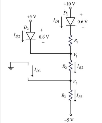
Figure 3
In Figure 3, the Diode
That is,
Therefore, the current following through diode
From Figure 1, the voltage at node
Therefore, the node voltage,
Apply Kirchhoff’s current law at node
Substitute
Calculate the current
Substitute
Therefore, the current following diode
Calculate the current following through resistor,
Substitute
Apply Kirchhoff’s current law at node
Substitute
Want to see more full solutions like this?
Chapter 2 Solutions
Microelectronics: Circuit Analysis and Design


- How is a solid-state diode tested? Explain.arrow_forwardaccepting that D1 and D2 diodes have the same properties in the circuit given in the figurea) output voltage, b) current flowing through the resistor,c) current flowing from diodes calculate.arrow_forwardIn the circuit shown in Figure 2–52 (p. 97), the Zener diode has a reverse breakdown voltage of 12V. RS = 50 Ohms, VS = 20V, and RL can vary from 100 Ohms to 200 Ohms. Assuming that the Zener diode remains in breakdown, find: (a) the minimum and maximum current in the Zener diode; (b) the minimum and maximum power dissipated in the diode; and (c) the minimum rated power dissipation that RS should have.arrow_forward
- For the circuit shown in Figure 2-a, plot the output voltage across the resistance R, using the diode characteristic presented in Figure 2-b. Assume the input AC voltage supply given by Vs = 1. sin(2pifot). Where fo = 100 Hz. In addition, could you suggest a method on how to keep the output voltage more constant.arrow_forwardA drift current density of 120A/cm2 is established in n-type silicon with an applied electric field of 18V/cm. If the electron and hole mobilities are µn =1250 cm2/V-s and µp =450 cm2/V-s, respectively, determine the required doping concentration. 2.5M 2. The circuit in figurearrow_forwarda. Using standard resistor values, what value of R1 is needed to achieve 1.18V ±0.01V at Vout? b. Using the R1 value chosen in (a) part, what happens to the voltage Vout when a load resistance of 10K is added (between Vout and ground). c. What is the minimum value of load resistance required for correct operation Zener diode is used in place of si diode. Or you can assume zener current according to requirement Answer it i will ratearrow_forward
- 2b) A regulator curcuit needs to be designed with an input power supply which has a nominal value of V_PS=20 V and can vary by ± %25 and nominal output voltage of 10 volts. For this purpose a zener diode is employed with specifications given; power rating of 1 W, 10V drop at Iz=25 mA, output load current is to vary between I(subscript L)=0-20 mA and zener resistance of r_Z=5Ω i) If the minimum Zener current is to be I_Z=5 mA, determine the required R_S ii) Determine the maximum variation in output voltage iii) Determine the regulation percentarrow_forwardWe wish to design a Si p+-n diode such that the avalanche breakdown and punchtrough at 300 K both occur at 15 V. Assume the relative dielectric constant of the semiconductor is 10, V0 is 0.5 and the breakdown field is 1 MV/cm. Determine the width and doping of the n-region.arrow_forwardDiodesFill in the blanks with the words belowcheck valve, conductance, convert, crystalline, impurities, infinite, galena, p–n junction, rectifying,resistance, selenium, semiconductor, switching circuits, tailored, temperature, threshold, two-terminal,unidirectionalA diode is a 1 ………………… electronic component that conducts current primarily in one direction(asymmetric 2 ………………..); it has low (ideally zero) 3 ……………… in one direction, and high (ideally4 ………………..) resistance in the other. A 5 ………….. diode, the most common type today, is a 6……….. piece of semiconductor material with a 7 ………………. connected to two electrical terminals. Avacuum tube diode has two electrodes, a plate (anode) and a heated cathode. Semiconductor diodes were thefirst semiconductor electronic devices. The discovery of crystals' 8 ……………… abilities was made byGerman physicist Ferdinand Braun in 1874. The first semiconductor diodes, developed around 1906, weremade of mineral crystals such as 9 ……………….. . Today,…arrow_forward
- For the values of R1=230, R2=230, R3=400, Vs=15. If the real diode (offset voltage=0.7V) were conduxting, then the value of voltage source Vb should be? solve correct or will dislikearrow_forwardThe applied electric field in p-type silicon is E=10V/cm. The semiconductor conductivity is 1.5(Ω-cm)-1and cross-sectional area is 10-5cm2. Determine the driftcurrent. (b) A drift current density of 120A/cm2is established in n-type silicon with an applied electric field of 18V/cm. If the electron and hole mobilities are µn =1250 cm2/V-s and µp =450 cm2/V-s, respectively, determine the required doping concentration.arrow_forwardWhile constructing a Bridge rectifier, the designer mistakenly has swapped the terminals of D3 as shown in the figure below, where • Diode D3 is damaged so that it is always open circuit regardless of the applied voltage. • vs(t) is a sinusoidal signal with a peak value (Vs = 5 V). • Diodes are modelled using the constant voltage model with VDO = 0.7 V • The ac line voltage has an rms value of 120 V and a frequency (f) = 60 Hz • The resistance RL = 10 kohm. a) Calculate the transformer turns ratio (N1/N2) if vs(t) is obtained from the secondary side of the transformer whose primary side is connected to the ac line voltage (which has a 120 V rms value). b) Plot in the same graph the input signal vs(t) and the output signal vout(t) (show all details including amplitudes, time instances, etc.) c) Calculate the rms values of the output signal vout(t). (hint: sin2 (x) = 0.5(1- cos(2x))) d) If a capacitor C = 3.58 µF is connected across R = 10 kohm, repeat (b) in a new graph e) With the…arrow_forward
