
Microelectronics: Circuit Analysis and Design
4th Edition
ISBN: 9780073380643
Author: Donald A. Neamen
Publisher: McGraw-Hill Companies, The
expand_more
expand_more
format_list_bulleted
Videos
Textbook Question
Chapter 2, Problem 2.9TYU
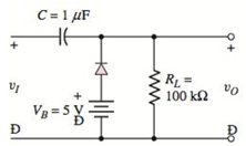
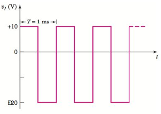
Determine the steady−state output voltage
Expert Solution & Answer
Want to see the full answer?
Check out a sample textbook solution
Students have asked these similar questions
Consider the circuit shown in Figure 2. The cut-in voltage of each diode is . Let and
assume both diodes are conducting. Determine if this is a valid assumption and
explain your answer. And calculate the values of IR, ID, Ip2, and V..
Rj =1.7 kQ
ww
VB =1 V
D1
Dz
R2D
4 kQ
Figure 2
In the circuit shown in the figure, diode voltages are given as 0.6V and rD = 100 ohms. When point B is open circuit AIf + 5V is applied to the point of application, drawing the shape of the circuit formed and calculating the currents passing through the resistors.calculate.
Consider the diode circuit shown below.
If Vs is a sinewave with a peak amplitude of 12 Volts at 60Hz, and diodes D1 & D2 are considered ideal, sketch the appearance of the waveform at node voltage Vout . Sketch the appearance of the waveform at Vout .
Chapter 2 Solutions
Microelectronics: Circuit Analysis and Design
Ch. 2 - Repeat Example 2.1 if the input voltage is...Ch. 2 - Consider the bridge circuit shown in Figure 2.6(a)...Ch. 2 - Assume the input signal to a rectifier circuit has...Ch. 2 - The input voltage to the halfwave rectifier in...Ch. 2 - Consider the circuit in Figure 2.4. The input...Ch. 2 - The circuit in Figure 2.5(a) is used to rectify a...Ch. 2 - The secondary transformer voltage of the rectifier...Ch. 2 - Determine the fraction (percent) of the cycle that...Ch. 2 - The Zener diode regulator circuit shown in Figure...Ch. 2 - Repeat Example 2.6 for rz=4 . Assume all other...
Ch. 2 - Consider the circuit shown in Figure 2.19. Let...Ch. 2 - Suppose the currentlimiting resistor in Example...Ch. 2 - Suppose the power supply voltage in the circuit...Ch. 2 - Design a parallelbased clipper that will yield the...Ch. 2 - Sketch the steadystate output voltage for the...Ch. 2 - Consider the circuit in Figure 2.23(a). Let R1=5k...Ch. 2 - Determine the steadystate output voltage O for the...Ch. 2 - Design a parallelbased clipper circuit that will...Ch. 2 - Consider the circuit shown in Figure 2.38, in...Ch. 2 - Consider the circuit shown in Figure 2.39. The...Ch. 2 - Repeat Example 2.11 for the case when R1=8k ,...Ch. 2 - The cutin voltage of each diode in the circuit...Ch. 2 - Prob. 2.12TYUCh. 2 - Consider the OR logic circuit shown in Figure...Ch. 2 - Consider the AND logic circuit shown in Figure...Ch. 2 - (a) Photons with an energy of hv=2eV are incident...Ch. 2 - Determine the value of resistance R required to...Ch. 2 - What characteristic of a diode is used in the...Ch. 2 - Prob. 2RQCh. 2 - Describe a simple fullwave diode rectifier circuit...Ch. 2 - Prob. 4RQCh. 2 - Prob. 5RQCh. 2 - Describe a simple Zener diode voltage reference...Ch. 2 - What effect does the Zener diode resistance have...Ch. 2 - What are the general characteristics of diode...Ch. 2 - Describe a simple diode clipper circuit that...Ch. 2 - Prob. 10RQCh. 2 - What one circuit element, besides a diode, is...Ch. 2 - Prob. 12RQCh. 2 - Describe a diode OR logic circuit. Compare a logic...Ch. 2 - Describe a diode AND logic circuit. Compare a...Ch. 2 - Describe a simple circuit that can be used to turn...Ch. 2 - Consider the circuit shown in Figure P2.1. Let...Ch. 2 - For the circuit shown in Figure P2.1, show that...Ch. 2 - A halfwave rectifier such as shown in Figure...Ch. 2 - Consider the battery charging circuit shown in...Ch. 2 - Figure P2.5 shows a simple fullwave battery...Ch. 2 - The fullwave rectifier circuit shown in Figure...Ch. 2 - The input signal voltage to the fullwave rectifier...Ch. 2 - The output resistance of the fullwave rectifier in...Ch. 2 - Repeat Problem 2.8 for the halfwave rectifier in...Ch. 2 - Consider the halfwave rectifier circuit shown in...Ch. 2 - The parameters of the halfwave rectifier circuit...Ch. 2 - The fullwave rectifier circuit shown in Figure...Ch. 2 - Consider the fullwave rectifier circuit in Figure...Ch. 2 - The circuit in Figure P2.14 is a complementary...Ch. 2 - Prob. 2.15PCh. 2 - A fullwave rectifier is to be designed using the...Ch. 2 - Prob. 2.17PCh. 2 - (a) Sketch o versus time for the circuit in Figure...Ch. 2 - Consider the circuit shown in Figure P2.19. The...Ch. 2 - Consider the Zener diode circuit shown in Figure...Ch. 2 - Consider the Zener diode circuit shown in Figure...Ch. 2 - In the voltage regulator circuit in Figure P2.21,...Ch. 2 - A Zener diode is connected in a voltage regulator...Ch. 2 - Consider the Zener diode circuit in Figure 2.19 in...Ch. 2 - Design a voltage regulator circuit such as shown...Ch. 2 - The percent regulation of the Zener diode...Ch. 2 - A voltage regulator is to have a nominal output...Ch. 2 - Consider the circuit in Figure P2.28. Let V=0 ....Ch. 2 - The secondary voltage in the circuit in Figure...Ch. 2 - The parameters in the circuit shown in Figure...Ch. 2 - Consider the circuit in Figure P2.31. Let V=0 (a)...Ch. 2 - Prob. 2.32PCh. 2 - Each diode cutin voltage is 0.7 V for the circuits...Ch. 2 - The diode in the circuit of Figure P2.34(a) has...Ch. 2 - Consider the circuits shown in Figure P2.35. Each...Ch. 2 - Plot O for each circuit in Figure P2.36 for the...Ch. 2 - Consider the parallel clipper circuit in Figure...Ch. 2 - A car’s radio may be subjected to voltage spikes...Ch. 2 - Sketch the steadystate output voltage O versus...Ch. 2 - Prob. D2.40PCh. 2 - Design a diode clamper to generate a steadystate...Ch. 2 - For the circuit in Figure P2.39(b), let V=0 and...Ch. 2 - Repeat Problem 2.42 for the circuit in Figure...Ch. 2 - The diodes in the circuit in Figure P2.44 have...Ch. 2 - In the circuit in Figure P2.45 the diodes have the...Ch. 2 - The diodes in the circuit in Figure P2.46 have the...Ch. 2 - Consider the circuit shown in Figure P2.47. Assume...Ch. 2 - The diode cutin voltage for each diode in the...Ch. 2 - Consider the circuit in Figure P2.49. Each diode...Ch. 2 - Assume V=0.7V for each diode in the circuit in...Ch. 2 - The cutin voltage of each diode in the circuit...Ch. 2 - Let V=0.7V for each diode in the circuit in Figure...Ch. 2 - For the circuit shown in Figure P2.54, let V=0.7V...Ch. 2 - Assume each diode cutin voltage is V=0.7V for the...Ch. 2 - If V=0.7V for the diode in the circuit in Figure...Ch. 2 - Let V=0.7V for the diode in the circuit in Figure...Ch. 2 - Each diode cutin voltage in the circuit in Figure...Ch. 2 - Let V=0.7V for each diode in the circuit shown in...Ch. 2 - Consider the circuit in Figure P2.61. The output...Ch. 2 - Consider the circuit in Figure P2.62. The output...Ch. 2 - Prob. 2.63PCh. 2 - Consider the circuit shown in Figure P2.64. The...Ch. 2 - The lightemitting diode in the circuit shown in...Ch. 2 - The parameters of D1 and D2 in the circuit shown...Ch. 2 - If the resistor in Example 2.12 is R=2 and the...Ch. 2 - Consider the photodiode circuit shown in Figure...Ch. 2 - Consider the fullwave bridge rectifier circuit....Ch. 2 - Design a simple dc voltage source using a...Ch. 2 - A clipper is to be designed such that O=2.5V for...Ch. 2 - Design a circuit to provide the voltage transfer...
Knowledge Booster


Learn more about
Need a deep-dive on the concept behind this application? Look no further. Learn more about this topic, electrical-engineering and related others by exploring similar questions and additional content below.Similar questions
- Sketch i agains v to scale for the circuit. Assume 0.6 V for all diodes in the forward-bias region.arrow_forwardConsider a silicon pn junction diode at T 300K. The reverse saturation current is Is = 10-14 A and the ideality factor n = 1. Determine the diode current for a diode voltage of VD = 0.573 V and use that to determine the DC and AC resistance of the diode. RDC = 14.13 k rac = 639 Q RDC = 234 Q2 = rac=8Q RDC = 7.00 KQ rac = 307 Q RDC = 1.43 kQ rac = 58 Qarrow_forwardDetermine the diode current (in Ampere) at 70°C for a silicon diode with reverse saturation current 70 nanoAmpere and an applied forward bias of 0.8 volts. The constant k value is: The Temperature (in Kelvin) is: The Diode current (in Ampere) is:arrow_forward
- A. Determine the peak forward current through each diode in Figure 2. B. Determine the output voltage waveform for each circuit in Figure 2. 22k0 22kn +30V +30 V Ov V. ov 12v 12V. -30V -30 V (b) 22k +30V +30 V ov V. ov 12V 12V 30V -30 V (c) (4)arrow_forwardDraw the input waveform and output waveform for the circuit given below with proper values marked in the figure. Assume D1 as germanium and D2 as silicon diodes. Input Vpp%3D20V, V1=3 V and V2=10 V. R D2 D1 Vin Vout V1 V2 Maximum voltage of output waveform Minimum voltage of output waveform Psarrow_forward. If a 480 ?F capacitor is added to the output in Figure 2.1, calculate the following:i. Vripple.ii. Average voltage, Vdc.iii. Sketch a graph of the input and output voltage against time of the capacitor.(Built-in-potential of silicon = 0.7V)arrow_forward
- Calculate the current flowing through the given circuit and the voltage value at the V0 ends. (Threshold voltage = 0.3V for Germanium diodes, Threshold voltage for silicon diodes = 0.6V)arrow_forwardIn RL load connected (without free transition diode), single phase, uncontrolled, full wave rectifier (4 diodes), the source voltage is sinusoidal and its effective value is 44Volt, 50 Hz. The ohmic load value connected to the circuit is 10 ohms. Average value of load current calculate. (L>>R) a) 4.16 A b) 3.46 A C) 3.26A d) 4.56 A e) 3.96 Aarrow_forwardConsider the circuit with three diodes and a AC input, as shown below: D2 R1 D1 D3 R2 Assume that the input AC voltage is Ttsin(100TTT). You may consider the diodes to be ideal. mean voltage generated across resistor R2 is (assuming current direction to be from AC so into R1, through diode network, and through R2 from top to bottom): O a. 0.5V Ob. -0.5V O c. 1V O d. OVarrow_forward
- 0:- Consider the circuit in Figure a) What type of circuit is this? b) Find and Sketch the voltage waveform across RL, assume the diodes are practical. c) If 100uf capacitor parallel with the resistor, calculate the ripple is connected factor I O o Darrow_forwardA. In your own words and with the aid of suitable diagrams, describe the following: a) The zener diode and its characteristics. b) Design a limitter circuit using diodes to limit the output voltage to 4.7V during the positive signwave and to -6.7V in the negative signwave. B. Consider the following circuit. Suppose that diode D1 is ideal. a) Give the state of the diode D1: conductive or blocking. Explain. b) Calculate the current flowing through D1. c) Calculate the voltage VR2 across the resistance R2. 1kQ D1 R1 R2 1) ImA 10V 4KQ C. In the circuit shown below the knee current for the ideal Zener diode is 10 mA. Calculate the minimum value of load resistance RL in order to maintain 5 volts across the load resistance RL. 1002 IL 10V V, = 5V A Rarrow_forward1. Draw the three (3) Equivalent Circuit of a Diode. 2. Determine the diode current (in Ampere) at 90°C for a silicon diode with reverse saturation current of 60 nanoAmpere and an applied forward bias of 0.8 volts. The constant k value is: The Temperature (in Kelvin) is: The Diode current (in Ampere) is:arrow_forward
arrow_back_ios
SEE MORE QUESTIONS
arrow_forward_ios
Recommended textbooks for you

19 Power Diodes | Power Electronics; Author: Walid Issa Plus;https://www.youtube.com/watch?v=_E-4bIYlNYQ;License: Standard Youtube License