
Videos
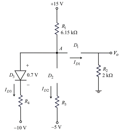
The cut−in voltage of each diode in the circuit shown in Figure P2.52 is Vγ=0.7V . Determine ID1,ID2,ID3 , and VA for (a) R3=14 kΩ,R4=24 kΩ ; (b) R3=3.3 kΩ,R4=5.2 kΩ ; and (c) R3=3.3 kΩ,R4=1.32 kΩ .
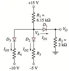
Figure P2.52
(a)
The values of ID1,ID2,ID3, and VA
Answer to Problem 2.52P
The current flowing through diodes is
ID3=0.5 mA
ID2=0.5 mA , ID1=1 mA and VA=2.7 V
Explanation of Solution
Given:
R3=14kΩ R4=24kΩ
Calculation:
The cut-in voltage for each diode is, Vγ=0.7V
Assume all diodes are ON.
Draw the circuit diagram with node voltages and cut-in voltages.
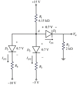
Apply Kirchhoff’s current law node A.
VA−156.15k+VA−0.72k+VA−0.7−(−5)R3+VA−0.7−(−10)R4=0VA−156.15k+VA−0.72k+VA+4.3R3+VA+9.3R4=0
Substitute 14 kΩ for R3 and 24 kΩ for R4 .
VA−156.15k+VA−0.72k+VA+4.314k+VA+9.324k=0VA−156.15+VA−0.72+VA+4.314+VA+9.324=0(16.15+12+114+124)VA−156.15−0.72+4.314+9.324=00.7756VA−2.094=0VA=2.7 V
Therefore, the voltage at node A, VA is 2.7 V
Calculate the current flowing through diode, D1 .
ID1=VA−0.72k
Substitute 2.7V for VA .
ID1=2.7−0.72k=22k=1 mA
Therefore, the current flowing through diode D1, is ID1=1 mA .
Calculate the current flowing through diode, D2 .
ID2=VA−0.7−(−5)R3
Substitute 2.7V for VA and 14 kΩ for R3 .
ID2=2.7−0.7+514k=714k=0.5 mA
Therefore, the current flowing through diode D2, is ID2=0.5 mA .
Calculate the current flowing through diode, D3 .
ID3=VA−0.7−(−10)R4
Substitute 2.7V for VA and 24 kΩ for R4 .
ID3=2.7−0.7+1024k=1224k=0.5 mA
Therefore, the current flowing through diodes is ID3=0.5 mA
Conclusion:
Therefore, the current flowing through diodes is
ID3=0.5 mA
ID2=0.5 mA , ID1=1 mA and VA=2.7 V
(b)
The values of ID1,ID2,ID3, and VA
Answer to Problem 2.52P
The current flowing through diodes is VA=−0.991V , ID1= 0 A , ID2=1.003 mA and ID3=1.6 mA
Explanation of Solution
Given:
R3=3.3kΩ R4=5.2kΩ
Calculation:
Assume diode D1 is OFF and remaining diodes are ON.
Draw the circuit diagram with node voltages and cut-in voltages.
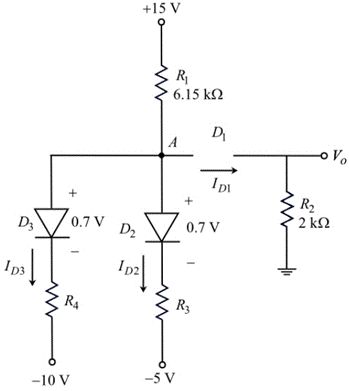
Apply Kirchhoff’s current law node A.
VA−156.15k+VA−0.7−(−5)R3+VA−0.7−(−10)R4=0VA−156.15k+VA+4.3R3+VA+9.3R4=0
Substitute 3.3 kΩ for R3 and 5.2 kΩ for R4 .
VA−156.15k+VA+4.33.3k+VA+9.35.2k=0VA−156.15+VA+4.33.3+VA+9.35.2=0(16.15+13.3+15.2)VA−156.15+4.33.3+9.35.2=00.6579VA+0.6525=0VA=−0.65250.6579=−0.991V
Therefore, the voltage at node A, VA is −0.991V
The diode D1 is reverse biased. Therefore, the current flowing through diode D1 is zero.
That is, ID1=0 A .
Therefore, the current flowing through diode D1,
ID1= 0 A
Calculate the current flowing through diode, D2 .
ID2=VA−0.7−(−5)R3
Substitute −0.991V for VA and 3.3 kΩ for R3 .
ID2=−0.991−0.7+53.3k=3.3093.3k=1.003 mA
Therefore, the current flowing through diode D2, is ID2=1.003 mA .
Calculate the current flowing through diode, D3 .
ID3=VA−0.7−(−10)R4
Substitute −0.991V for VA and 5.2 kΩ for R4 .
ID3=−0.991−0.7+105.2k=8.3095.2k=1.6 mA
Therefore, the current flowing through diode D3, is ID3=1.6 mA .
Conclusion:
Therefore, the current flowing through diodes is VA=−0.991V , ID1= 0 A , ID2=1.003 mA and ID3=1.6 mA
(c)
The values of ID1,ID2,ID3, and VA
Answer to Problem 2.52P
The current flowing through diodes is VA=−5V , ID1=0 A , ID2=0 A
ID3=3.25 mA
Explanation of Solution
Given:
R3=3.3kΩR4=1.32kΩ
Calculation:
Assume diode D1 and D2 are OFF and diode D3 is ON.
Draw the circuit diagram with node voltages and cut-in voltages.
Apply Kirchhoff’s current law node A.
VA−156.15k+VA−0.7−(−10)R4=0VA−156.15k+VA+9.3R4=0
Substitute 1.32 kΩ for R4 .
VA−156.15k+VA+9.31.32k=0VA−156.15+VA+9.31.32=0(16.15+11.32)VA−156.15+9.31.32=00.92VA+4.606=0VA=−5V
Therefore, the voltage at node A, VA is −5V .
The Diode D1 and D2 are reverse biased. Therefore, the current flowing through diode D1 is zero.
That is, ID1=0 A .
Therefore, the current flowing through diode D1,ID1 is 0 A.
The current flowing through the diode, D2 is zero.
That is,
ID2=0 A.
Therefore, the current flowing through diode D2,ID2 is 0 A.
Calculate the current flowing through diode, D3 .
ID3=VA−0.7−(−10)R4
Substitute −5V for VA and 1.32 kΩ for R4 .
ID3=−5−0.7+101.32k=4.31.32k=3.25 mA
Therefore, the current flowing through diode D3, is ID3=3.25 mA .
Conclusion:
Therefore, the current flowing through diodes is VA=−5V , ID1=0 A , ID2=0 A
ID3=3.25 mA
Want to see more full solutions like this?
Chapter 2 Solutions
Microelectronics: Circuit Analysis and Design


- 1. Determine the z-transform, including the region of convergence (ROC), of the following signals: a)x[n={3,0,0,0,0,51-4} b) x2[n] = ((1/3)^n ,n ≥0 2", n < 0 c) X3[n]= (1/3)^n- 2", n ≥ 0 0, n < 0arrow_forwardUse ECL configuration to realize a 2-inputs OR /NOR gate and verify its function using the truth table, showing the state of each transistor in the circuit. Assume Vcc 5V, VEE-0V & VREF=1.5V.arrow_forwardTwenty-five signals, ten of them have 3.4 kHz bandwidth, the other have bandwidth of 5 kHz are FDM/TDM multiplexed then modulated by an RF carrier of 800 kHz using AM modulator: Calculate minimum multiplexing and transmission bandwidths. Calculate the guard band (BWGuard) to be added between each two signals and below the first one to result a multiplexing bandwidth of 131.5 kHzarrow_forward
- An FDM is used to multiplex two groups of signals using AM-SSB, the first group contains 25 speech signals, each has maximum frequency of 4 kHz, the second group contains 15 music signals, each has maximum frequency of 10 kHz. A guard bandwidth of 500 Hz is used between each two signals and before the first one. 1. Find the BWmultiplexing 2. Find the BWtransmission if the multiplexing signal is modulated using AM-DSB-LC.arrow_forwardA single tone is modulated using FM transmitter. The SNR; at the input of the demodulator Is 20 dB. If the maximum frequency of the modulating signal is 4 kHz, and the maximum frequency deviation is 12 kHz, find the SNR, and the bandwidth (using Carson rule) at the following conditions: 1. For the given values of fm and Af. 2. If the amplitude of the modulating signal is increased by 80%. 3. If the amplitude of the modulating signal is decreased by 50%, and frequency of modulating signal is increased by 50%.arrow_forwardFM station of 100 MHz carrier frequency modulated by a 20 kHz sinusoid with an amplitude of 10 volt, so that the peak frequency deviation is 25 kHz determine: 1) The BW of the FM signal. 2) The approximated BW if the modulating signal amplitude is increased to 50 volt. 3) The approximated BW if the modulating signal frequency is increased by 70%. 4) The amplitude of the modulating signal if the BW is 65 kHz.arrow_forward
- b) The joint probability function for the random variables X and Y is given in Table below. Find a) the marginal probability function of X and Y. P(Y/X) and P(X/Y). c) P(X ≥ 2, Y ≤ 2) y 1 2 3 10.05 0.05 0.1 P(X, Y) = X 20.05 0.1 0.35 3 0 0.2 0.1arrow_forwardSuppose a random variable X as pmf / Px (x) = { %, x = 1, 2, 3, 0, otherwise. find constand c ①P(X = 1), P(X 7,2), PC1 3) C CDFarrow_forwardSuppose that a coin is tossed three so that the sample space is Let X represent the number of heads that can come up. i) Find the probability function corresponding to the random variable X. Assuming that the coin is fair ii) Find the distribution function for the random variable X. iii) Obtain its graph.arrow_forward
- Q9 A single-phase transformer, 2500 / 250 V, 50 kVA, 50 Hz has the following parameters, the Primary and secondary resistances are 0.8 ohm and 0.012 ohm respectively, the primary and secondary reactance are 4 ohm and 0.04 ohm respectively and the transformer gives 96% maximum efficiency at 75% full-load. The magnetizing component of-load current is 1.2 A on 2500 V side. 1- Draw the equivalent circuit referred to primary (H.V side) and inserts all the values in it 2- Find out Ammeter, voltmeter and wattmeter readings on open-circuit and short-circuit test. If supply is given to 2500 V side in both cases. Ans. O.C. Test (Vo= 2500 V, lo=1.24 A, Wo=781.25 w) S.C. Test (Vsc =164.924 V, Isc =20 A, Wsc =800 w )arrow_forwardQ2-A)- Enumerate the various losses in transformer. Explain how each loss varies with (Load current, supply voltage). B)- Draw the pharos diagram at load on primary side.arrow_forwardQ2- What are the parameters and loss that can be determined during open-circuit test of singlephase transformer. Draw the circuit diagram of open-circuit test and explain how can you calculate the Parameters and loss.arrow_forward
 Introductory Circuit Analysis (13th Edition)Electrical EngineeringISBN:9780133923605Author:Robert L. BoylestadPublisher:PEARSON
 Delmar's Standard Textbook Of ElectricityElectrical EngineeringISBN:9781337900348Author:Stephen L. HermanPublisher:Cengage Learning
 Programmable Logic ControllersElectrical EngineeringISBN:9780073373843Author:Frank D. PetruzellaPublisher:McGraw-Hill Education
 Fundamentals of Electric CircuitsElectrical EngineeringISBN:9780078028229Author:Charles K Alexander, Matthew SadikuPublisher:McGraw-Hill Education
 Electric Circuits. (11th Edition)Electrical EngineeringISBN:9780134746968Author:James W. Nilsson, Susan RiedelPublisher:PEARSON
 Engineering ElectromagneticsElectrical EngineeringISBN:9780078028151Author:Hayt, William H. (william Hart), Jr, BUCK, John A.Publisher:Mcgraw-hill Education,