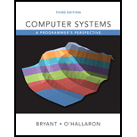
Computer Systems: A Programmer's Perspective (3rd Edition)
3rd Edition
ISBN: 9780134092669
Author: Bryant, Randal E. Bryant, David R. O'Hallaron, David R., Randal E.; O'Hallaron, Bryant/O'hallaron
Publisher: PEARSON
expand_more
expand_more
format_list_bulleted
Question
Chapter 4.3, Problem 4.21PP
Program Plan Intro
Processing stages:
- The processing of an instruction has number of operations.
- The operations are organized into particular sequence of stages.
- It attempts to follow a uniform sequence for all instructions.
- The description of stages are shown below:
- Fetch:
- It uses program counter “PC” as memory address to read instruction bytes from memory.
- The 4-bit portions “icode” and “ifun” of specifier byte is extracted from instruction.
- It fetches “valC” that denotes an 8-byte constant.
- It computes “valP” that denotes value of “PC” plus length of fetched instruction.
- Decode:
- The register file is been read with two operands.
- It gives values “valA” and “valB” for operands.
- It reads registers with instruction fields “rA” and “rB”.
- Execute:
- In this stage the ALU either performs required operation or increments and decrements stack pointer.
- The resulting value is termed as “valE”.
- The condition codes are evaluated and destination register is updated based on condition.
- It determines whether in a jump instruction a branch should be considered or not.
- Memory:
- The data is been written to memory or is been read from the memory in this stage.
- The value that is read is determined as “valM”.
- Write back:
- The results are been written to register file.
- It can write up to two results.
- PC update:
- The program counter “PC” denotes memory address to read bytes of instruction from memory.
- It is used to set next instruction’s address.
- Fetch:
Combinational circuits and HCL expressions:
- The computational blocks are been constructed by accumulating several logic gates into network.
- The restrictions are been shown below:
- Each of input for logic gate should be associated to any one shown below:
- One of system inputs, that is identified as primary inputs.
- Output connection for some element in memory.
- Output of some logic gate.
- Outputs obtained from more than two logic gates could not be linked together.
- The wire would be driven to different voltages.
- It can cause malfunction in circuit.
- The network should not contain cycles.
- The loops in circuit can cause ambiguity in function
computed by network.
- The loops in circuit can cause ambiguity in function
- Each of input for logic gate should be associated to any one shown below:
- The “HCL” denotes a hardware control language that is used for describing control logic of different processor designs.
Expert Solution & Answer
Want to see the full answer?
Check out a sample textbook solution
Students have asked these similar questions
Are these instruction true or false ?why? (choose five only
LDI R13, 0x20 (1
.Harvard architecture consist of separate memories (2
MOV CS, AX (3
[MOV AL,[BX (4
To configure port B as output (5
LDI R16, OXFF*
OUT DDRC, R16
To read the content of port C (6
LDI R20, 0x00
OUT DDRC, R20
Question: C part
A Instruction Set Architecture
A.1 Instruction set
We present a list of instructions typical of a RISC (reduced instruction set computer) machine. In data-movement and control instructions, the addresses may be immediate #X, direct (memory) M, indirect (memory) [M], register r, or register indirect [r] addresses. Data-processing instructions use immediate or register addressing. PC is the programme counter and a <- b indicates that the value of b is placed in a.
LOAD a, b a <- b
STOR a, b a <- b
ADD a, b, c a <- b + c
ASH a, b, c a <- (b >>[s] c)
LSH a, b, c a <- (b >>[u] c) BR a PC <- a
SUB
a,
b,
c
a
<-
b
- c
BEQ
a,
b,
c
PC
<-
a
if
b =
c
MUL
a,
b,
c
a
<-
b
* c
BNE
a,
b,
c
PC
<-
a
if
not
b = c
DIV
a,
b,
c
a
<-
b…
(e) Instruction(s) to copy contents at one memory location to another: C[g] =A[i+j-3). Assume i, j,g values are in registers x5, x6, x7. Assume base address in memory of Array data structures 'A, B' (or address in memory of 'A[O]' and 'B[O]') are stored in Registers x28, 29• In RISCV, only load and store instructions access memory locations • These instructions must follow a 'format' to access memory • Assume a 32 bit machine in all problems unless asked to assume otherwise
Chapter 4 Solutions
Computer Systems: A Programmer's Perspective (3rd Edition)
Ch. 4.1 - Prob. 4.1PPCh. 4.1 - Prob. 4.2PPCh. 4.1 - Prob. 4.3PPCh. 4.1 - Prob. 4.4PPCh. 4.1 - Prob. 4.5PPCh. 4.1 - Prob. 4.6PPCh. 4.1 - Prob. 4.7PPCh. 4.1 - Prob. 4.8PPCh. 4.2 - Practice Problem 4.9 (solution page 484) Write an...Ch. 4.2 - Prob. 4.10PP
Ch. 4.2 - Prob. 4.11PPCh. 4.2 - Prob. 4.12PPCh. 4.3 - Prob. 4.13PPCh. 4.3 - Prob. 4.14PPCh. 4.3 - Prob. 4.15PPCh. 4.3 - Prob. 4.16PPCh. 4.3 - Prob. 4.17PPCh. 4.3 - Prob. 4.18PPCh. 4.3 - Prob. 4.19PPCh. 4.3 - Prob. 4.20PPCh. 4.3 - Prob. 4.21PPCh. 4.3 - Prob. 4.22PPCh. 4.3 - Prob. 4.23PPCh. 4.3 - Prob. 4.24PPCh. 4.3 - Prob. 4.25PPCh. 4.3 - Prob. 4.26PPCh. 4.3 - Prob. 4.27PPCh. 4.4 - Prob. 4.28PPCh. 4.4 - Prob. 4.29PPCh. 4.5 - Prob. 4.30PPCh. 4.5 - Prob. 4.31PPCh. 4.5 - Prob. 4.32PPCh. 4.5 - Prob. 4.33PPCh. 4.5 - Prob. 4.34PPCh. 4.5 - Prob. 4.35PPCh. 4.5 - Prob. 4.36PPCh. 4.5 - Prob. 4.37PPCh. 4.5 - Prob. 4.38PPCh. 4.5 - Prob. 4.39PPCh. 4.5 - Prob. 4.40PPCh. 4.5 - Prob. 4.41PPCh. 4.5 - Prob. 4.42PPCh. 4.5 - Prob. 4.43PPCh. 4.5 - Prob. 4.44PPCh. 4 - Prob. 4.45HWCh. 4 - Prob. 4.46HWCh. 4 - Prob. 4.47HWCh. 4 - Prob. 4.48HWCh. 4 - Modify the code you wrote for Problem 4.47 to...Ch. 4 - In Section 3.6.8, we saw that a common way to...Ch. 4 - Prob. 4.51HWCh. 4 - The file seq-full.hcl contains the HCL description...Ch. 4 - Prob. 4.53HWCh. 4 - The file pie=full. hcl contains a copy of the PIPE...Ch. 4 - Prob. 4.55HWCh. 4 - Prob. 4.56HWCh. 4 - Prob. 4.57HWCh. 4 - Our pipelined design is a bit unrealistic in that...Ch. 4 - Prob. 4.59HW
Knowledge Booster
Similar questions
- (a) Draw pipeline diagram (FI, DI, FO, EI) with one memory port for the following instructions: MOV [1234], 035 ADD_[1234], AX SUB BX, CX XOR CX, BX AND BX, 035 PUSH CX (b) Write the code for the following. Rewrite the code to reduce hazards by instruction rescheduling: [c] = [a] -[e] [b]= [c] + [d] [f] = [d] + [e]arrow_forward(a) Generate a full RTN code in Fetch, Decode, Execute and Write Back step for: MUL 602, #5, #2 Assume that, in this instruction, the registers used to temporarily store the fetched data are RI and R2. The result of arithmetic operation is stored temporarily in R3 before it being stored back in memory location M[602]. The initial Program Counter value is 500. The illustration is as in Figure Q41(a). Memory CPU Register 500 0600 0500 PC 501 0601 IR R1 R2 600 0005 R3 601 0003 602 Figure Q41(a)arrow_forward(c) The following Sigma 16 program has been loaded into memory at address 0000: load R3,y[RO] load R4,x[RO] lea R5, 2[RO] sub R1,R4,R3 mul R2,R1,R5 store R2,w[RO] trap RO,RO,RO x data 10 y data 12 w data 0 Show the content of the memory writing hexadecimal representation and using a table with 3 columns: the memory address, the contents of that memory address, and an explanation of what "the content (of that memory address) means". As a reference, here are the opcodes for RRR instructions: add 0, sub 1, mul 2, trap c. And here the opcodes for RX instructions: lea 0, load 1, store 2. [7]arrow_forward
- B. (15%) Consider the datapath for the execution of the instruction beq $t0, $t1, 100 Draw a Datapath diagram to show the execution of the instruction.arrow_forwardQ4) A- Write an assembly program to move (N) memory contents located at starting address with offset (AFOH) to the new location address starting at offset (500h). B- Show (for both 1 and 2) the content of CL register, OF, SF, ZF, and CF after execution the following sequence of instruction: 1-MOV AL , 85 2- MOV AL, - 52 MOV CL, 70 MOV CL,-9 ADD CL, AL ADD CL, AL Is the result correct, why?arrow_forwardQ2) Write an assembly language program to monitor the physical digitized quantity come from port 8080h and if it is greater than 40h the processer sets the valve connected to the port A00AH on bit 2 and otherwise resets it. Q3) If BP-1000, DS=0400, SS-0700, Cs-0500 and AL-EDH, for the following instruction: MOV [BP] + 1234H, AL Find the physical address in the memory. Q4) For the above question, if BX is used instead of BP, what is the physical address in the memory?arrow_forward
- (a) An instruction at address 021 in the basic computer has I-0, an operation code of the AND instruction, and an address part equal to 083 (all numbers are in hexadecimal). The memory word at address 083 contains the operand B8F2 and the content of AC is A937. Go over the instruction cycle and determine the contents of the following registers at the end of the execute phase: PC, AR, DR, AC, and IR. Repeat the problem six more times starting with an operation code of another memory- reference instruction.arrow_forwardQ4) Are these instruction true or false ?why?(choose five only) 1) LDI R13 , 0x20 2) Harvard architecture consist of separate memories. 3) MOV Cs, AX 4) MOV AL, [BX] 5) To configure port B as output LDI R16, OXFF OUT DDRC, R16 6) To read the content of port C LDI R20, 0x00 OUT DDRC, R20arrow_forward(c) Write a subroutine to copy the content of register R0 and R1 into the register R20 and R21 respectively. Initialize the Stack pointer to the last location of the RAM and preserve the content of the register R20 and R21 using the stack during the subroutine call. Illustrate the content of the stack and the stack pointer during the subroutine execution.arrow_forward
- (1) Compare Conditional and Control flags. (i1) Consider the instruction SUB AL, CL. (AL) = 50 H, (CL) = 20 H. Write the flaa register value (in Hex) after the execution of the instruction. Assume all the control flags are reset. (Note : Solve the question in paper, scan and upload along with the other Part B and C answers)arrow_forwardQuestion 1 (> For the first 14 questions, use the MIPS assembly code: SW $22, 40 ($24). AND $8, $17, $18 ADDI $20, $12, 5 OR $16, $10, $11 Each register contains an initial value of decimal 100 plus its register number. (e.g. register $8 contains 108, register $22 contains 122, etc). The code begins running on a 5-stage MIPS pipelined processor with SW starting in cycle 1. Diagram the instructions within a pipeline diagram to determine which stage each instruction will be in during each cycle. Then answer the next 14 questions, During cycle 3, which instruction will use values from the IF/ID pipeline register? Question 2 During cycle 4, which instruction will use values from the ID/EX pipeline register? Question 3 During cycle 4, what decimal register number will be obtained from ID/EX.RegisterRs? Question 4 During cycle 4, which instruction will use values from the EX/MEM pipeline register? Question 5 ( During cycle 4, what decimal value is obtained from EX/MEM.ALUresult ?arrow_forward[2] ( Explain for each line why you chose a certain suffix such as b,w,l or q For each of the following lines of assembly language, determine the appropriate instruction suffix based on the operands. (For example, mov can be rewritten as movb, movw, movl, or movq.) mov mov mov που mov mov %oax, (%rsp) (%rax), %dx $0xFF, %bl (%rap,%rdx, 4), %d1 %rdx), %rax %dx, (%rax)arrow_forward
arrow_back_ios
SEE MORE QUESTIONS
arrow_forward_ios
Recommended textbooks for you
 Database System ConceptsComputer ScienceISBN:9780078022159Author:Abraham Silberschatz Professor, Henry F. Korth, S. SudarshanPublisher:McGraw-Hill Education
 Starting Out with Python (4th Edition)Computer ScienceISBN:9780134444321Author:Tony GaddisPublisher:PEARSON
 Digital Fundamentals (11th Edition)Computer ScienceISBN:9780132737968Author:Thomas L. FloydPublisher:PEARSON
 C How to Program (8th Edition)Computer ScienceISBN:9780133976892Author:Paul J. Deitel, Harvey DeitelPublisher:PEARSON
 Database Systems: Design, Implementation, & Manag...Computer ScienceISBN:9781337627900Author:Carlos Coronel, Steven MorrisPublisher:Cengage Learning
 Programmable Logic ControllersComputer ScienceISBN:9780073373843Author:Frank D. PetruzellaPublisher:McGraw-Hill Education

Database System Concepts
Computer Science
ISBN:9780078022159
Author:Abraham Silberschatz Professor, Henry F. Korth, S. Sudarshan
Publisher:McGraw-Hill Education

Starting Out with Python (4th Edition)
Computer Science
ISBN:9780134444321
Author:Tony Gaddis
Publisher:PEARSON

Digital Fundamentals (11th Edition)
Computer Science
ISBN:9780132737968
Author:Thomas L. Floyd
Publisher:PEARSON

C How to Program (8th Edition)
Computer Science
ISBN:9780133976892
Author:Paul J. Deitel, Harvey Deitel
Publisher:PEARSON

Database Systems: Design, Implementation, & Manag...
Computer Science
ISBN:9781337627900
Author:Carlos Coronel, Steven Morris
Publisher:Cengage Learning

Programmable Logic Controllers
Computer Science
ISBN:9780073373843
Author:Frank D. Petruzella
Publisher:McGraw-Hill Education