
Concept explainers
The currents
Answer to Problem 13.1EP
The currents are:
Explanation of Solution
Given:
The bias circuit and input stage portion of 741 op-amp circuit is shown below.
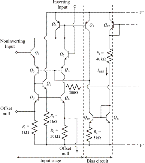
Figure 1
Resistance
Bias voltages are:
The base current is considered to be 0 A.
The base emitter voltages are:
Calculation:
Consider the given circuit. The formula for reference current that is established in the circuit branch consists of transistors
Transistors
Where,
Substitute the given values in the above equation.
By trial and error method,
For the given circuit, if the base current is neglected, then the collector current through transistors
Substituting the values,
Want to see more full solutions like this?
Chapter 13 Solutions
Microelectronics: Circuit Analysis and Design


- Please solve in detailarrow_forward6.7 The transmitting aerial shown in Fig. Q.3 is supplied with current at 80 A peak and at frequency 666.66 kHz. Calculate (a) the effective height of the aerial, and (b) the electric field strength produced at ground level 40 km away. 60 m Fig. Q.3 Input 48 m Eartharrow_forwardox SIM 12.11 Consider the class B output stage, using MOSFETs, shown in Fig. P12.11. Let the devices have |V|= 0.5 V and μC WIL = 2 mA/V². With a 10-kHz sine-wave input of 5-V peak and a high value of load resistance, what peak output would you expect? What fraction of the sine-wave period does the crossover interval represent? For what value of load resistor is the peak output voltage reduced to half the input? Figure P12.11 +5 V Q1 Q2 -5Varrow_forward
- 4 H ་་་་་་་ 四一周 A H₂ Find out put c I writ R as a function G, H, Harrow_forward4 H A H₂ 四一周 Find out put c I writ R as a function G, H, Harrow_forward8. (a) In a Round-Robin tournament, the Tigers beat the Blue Jays, the Tigers beat the Cardinals, the Tigers beat the Orioles, the Blue Jays beat the Cardinals, the Blue Jays beat the Orioles and the Cardinals beat the Orioles. Model this outcome with a directed graph. https://www.akubihar.com (b) (c) ✓ - Let G = (V, E) be a simple graph. Let R be the relation on V consisting of pairs of vertices (u, v) such that there is a path from u to vor such that u= v. Show that R is an equivalence relation. 3 3 Determine whether the following given pair of directed graphs, shown in Fig. 1 and Fig. 2, are isomorphic or not. Exhibit an isomorphism or provide a rigorous argument that none exists. 4+4=8 Աշ աշ ИНИЯ Fig. 1 Fig. 2 Querarrow_forward
- EXAMPLE 4.5 Objective: Determine ID, circuit. V SG' SD Vs and the small - signal voltage gain of a PMOS transistor Consider the circuit shown in Figure 4.20(a). The transistor parameters are A K = 0.80m- V Р _2’TP = 0.5V, and λ = 0 Varrow_forwardNeed a solution and don't use chatgptarrow_forwardNeed a solarrow_forward
 Introductory Circuit Analysis (13th Edition)Electrical EngineeringISBN:9780133923605Author:Robert L. BoylestadPublisher:PEARSON
 Delmar's Standard Textbook Of ElectricityElectrical EngineeringISBN:9781337900348Author:Stephen L. HermanPublisher:Cengage Learning
 Programmable Logic ControllersElectrical EngineeringISBN:9780073373843Author:Frank D. PetruzellaPublisher:McGraw-Hill Education
 Fundamentals of Electric CircuitsElectrical EngineeringISBN:9780078028229Author:Charles K Alexander, Matthew SadikuPublisher:McGraw-Hill Education
 Electric Circuits. (11th Edition)Electrical EngineeringISBN:9780134746968Author:James W. Nilsson, Susan RiedelPublisher:PEARSON
 Engineering ElectromagneticsElectrical EngineeringISBN:9780078028151Author:Hayt, William H. (william Hart), Jr, BUCK, John A.Publisher:Mcgraw-hill Education,