
Videos
Consider the simple MOS op−amp circuit shown in Figure P13.1. The biascurrent is
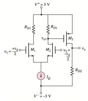
Figure P13.1
Want to see the full answer?
Check out a sample textbook solution
Chapter 13 Solutions
Microelectronics: Circuit Analysis and Design


- Determine VB, VE, VC, VCE, IB, IE, and IC in Figure. The 2N3904 is a general purpose transistor with a typical BDC 200 Vcc +30 V WWII VCE VB R₁ • 22 ΚΩ IC(mA) Chọn... * Chọn... * IB(UA) Chọn... * IE(MA) Chọn... ◆ Chọn... * Chọn... * Chọn... * VE VC R₂ ´ 10 ΚΩ www Rc 1.0 ΚΩ 2N3904 PDC=200 RE 1.0 ΚΩarrow_forwardThe Pinch off voltage for N- Channel JFET is -3V, maximum saturated drain current 8mA and the value of VGS is -1.5 V. Calculate drain current, a. 18 mA b. 2 mA c. 2.5 mA d. 4 mAarrow_forward4) Consider the clamping circuit below, assume Vref=3 V and Vin=5sin(wt) ..Draw the output voltage waveform. Clearly mark the max and min of the voltage.. Vrefarrow_forward
- The base-biased circuit in the figure is subjected to an increase in junction temperature from 25°C to 75°C. If βdc = 100 at 25°C and 150 at 75°C, Determine the base current Ib in microampere. Show complete solution. (Answer must in 2 decimal places)arrow_forwardSketch the de load line, quiescent collector current, quiescent voltsge, input power, output power and maximum efficiency of the circuit shown an Figure. The input results in a base current of 5 mA peak to peak What maximum output power can be delivered by the circuit, if the input voltage is changed resulting in a base current of 10mA peak to peak and hence find the maximum etficiency. cc=15 V R =18 2 -25arrow_forward........ (Figure-1) R. RB= 380kN,Rc= 1kN B = 100, VBB = Vcc=12V RB ww Vec CC ......... I, V CE СЕ V ВЕ BB Q-1-b) Describe briefly the input / output characteristics and application of Common Emitter BJT Configurationarrow_forward
- 45) We have buck converter, the maximum current of the inductor is Imax, the minimum inductor currentIs Imin. We now know the period of the switching signal is T=20 µs, the duty cycle D is 0.5, the load resistance R is 2 ohms, the input voltage is 30V, and the inductance L is 100 µH; What is Imax andIs Imin?arrow_forwardQuestion No. 2 a Inan experiment the voltage required for the device is 9V dc but unfortunately the transformer avai lable is of 220-6 V dc. Design a circuit which can power the device (use only methods that we have studied excluding Zener diode) b. Explain the behavior of the foll owing circuits if the input signal is triangular wave of peak voltage 5V and the biasing battery of 3V 4-arrow_forwardQ3) For the regulator circuit shown in figure below, Vin-15 V, Rs-10 2, Vz-9.1 V, VBE=0.8V, and R=40 2. What are the values of output voltage, input current, the load current, and collector current. 102016 2-8594 Vin R$ Ⓡ R₂ Voutarrow_forward
- The junction at a higher temperature in thermocouple is termed as: a) Transducer junction.b) High-temp junctionc) Hot junctiond) Compensation junctione) Thermos junctionarrow_forwardA) Design with drawing an Op-Amp series voltage regulator to give a regulated O/P voltage of 12V for an I/P of 15V B) Calculate the line regulation if the I/p increases to 4V leads to increase the O/P voltage to 0.02V.arrow_forwardProblem #6: An abrupt p-n junction varactor is used to tune an oscillator shown in Figure 3. At zero bias voltage, the varactor has a junction capacitance of 4pF, Vbi 1.3V for GaAs. The active device has CD = 2pF and RD = 10W. The load bias has L₁ = 15nH and R₁ = 10W. What are the oscillation frequencies at (a) -20V (b) -10V and (c) OV? = L₁ R₁ C₁ (V) -RD FIGURE-3 www CDarrow_forward
 Introductory Circuit Analysis (13th Edition)Electrical EngineeringISBN:9780133923605Author:Robert L. BoylestadPublisher:PEARSON
 Delmar's Standard Textbook Of ElectricityElectrical EngineeringISBN:9781337900348Author:Stephen L. HermanPublisher:Cengage Learning
 Programmable Logic ControllersElectrical EngineeringISBN:9780073373843Author:Frank D. PetruzellaPublisher:McGraw-Hill Education
 Fundamentals of Electric CircuitsElectrical EngineeringISBN:9780078028229Author:Charles K Alexander, Matthew SadikuPublisher:McGraw-Hill Education
 Electric Circuits. (11th Edition)Electrical EngineeringISBN:9780134746968Author:James W. Nilsson, Susan RiedelPublisher:PEARSON
 Engineering ElectromagneticsElectrical EngineeringISBN:9780078028151Author:Hayt, William H. (william Hart), Jr, BUCK, John A.Publisher:Mcgraw-hill Education,