
Videos
a.
Effective resistance
a.
Answer to Problem 14.40P
Value of effective resistance
Explanation of Solution
Given:
Bipolar diff-amp with active load and a pair of offset-null terminal is shown below.

Given parameters are:
Wipe arm of potentiometer is exactly at center.
Calculation:
As wipe arm of potentiometer is exactly at center. So,
As
So,
b.
Values of
b.
Answer to Problem 14.40P
Value of
Explanation of Solution
Given:
Bipolar diff-amp with active load and a pair of offset-null terminal is shown below.
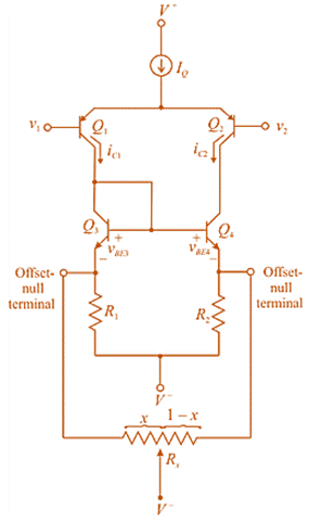
Given parameters are:
Calculation:
Now, KVL between terminals of
Here,
Now, on including the effect of potentiometer
The base emitter voltages are,
And
Substituting values from equation (4) and (5) in equation (1)
Now, substituting value from equation (2) and (3) in above equation,
Substituting the values
So,
Since,
So, to compensate the mismatches of transistor the value of
Want to see more full solutions like this?
Chapter 14 Solutions
Microelectronics: Circuit Analysis and Design


- Common-Emitter Configuration problem. Answer no. 24 only Reference: Electronic device and circuit theory 11th edition by Boylestadarrow_forwardcircuits 44 45arrow_forward1. For the circuits shown below, if A=∞, Calculate a) The overall input resistance, Rin b) The output resistance, Rout c) Overall voltage gain (vo/vs)arrow_forward
- For an efficient communication in PCM system, the number of samples per second must be at most be equal to twice the highest modulating frequency.a. A very important considerationb. No, it must be at least equal to twice the highest modulating frequencyc. 80-50 percent truearrow_forwardCOURSE: INDUSTRIAL ELECTRONICS DEGREE: BS ELECTRICAL ENGINEERING For a unijunction transistor with VBB = 20V, n = 0.65, RB1 ✓ 2K-ohms (IE = 0), and VD = 0.7, determine: a) RB2 b) RBB c) VRB1 d) VParrow_forwardanswer all A - Explain the relation of MOSFET input current and input impedance and their effect on the functionality of the device. B- Explain how to increase the efficiency of the solar cells (PV cells) through the integration of antennas. C- List three conditions need to be considered to choose a MOSFET for switching applications.arrow_forward
- Suppose a power supply is energized by an AC source of 119 V RMS. The transformer step-down ratio is 8:1, it uses a full-wave bridge rectifier circuit with silicon diodes, and the filter is nothing but a single electrolytic capacitor. Calculate the unloaded DC output voltage for this supply (assume 0.7 volts drop across each diode). Also, write an equation solving for DC output voltage (Vout), given all these parameters.arrow_forwardDerive the formulas before solving the unknowns. Round off to two decimal points. Enclosed your final answer into boxes.1.Draw the DC equivalent circuit.2.Draw the fixed bias base emitter circuit. Derive IB.3.Draw fixed bias collector emitter loop. Derive VCE.4.Solve for unknowns.arrow_forwardMultiple Choice directions: Circle the letter of the answers that best answer the question. 13. When using microwave tubes as amplifiers, what is used as bandpass filters? a. Transistors b. Oscillator c. All of the above d. Power tubes 14. The microstrip lines used to achieve maximum power transfer are intended for a. Signal coupling b. Decoupling to prevent feedback c. Low-noise amplification d. Impedance matching and tuning 15. A diode that when reverse biased will momentarily and will abruptly turn off. a. Varactor diode b. IMPATT c. Step recovery diodes d. PIN diodes 16. A microwave transmission line used to minimize noise and crosstalks. a. Stripline b. Hard line cable c. Waveguide d. Microstrip 17. The major difference between a low frequency transistors and microwave types is/are. a. B & C b. Packaging c. Material d. Internal geometry 18. Which of the following band belongs to the millimeter waves a. C b. Ku c. U d. L 19. Overcrowding in the frequency spectrum is prevalent…arrow_forward
- 1. (a) Determine the minimum acceptable value of Rs for the zener voltage regulator circuit shown inFigure 1. The zener specifications are: Vz = (14) V; Iz = (7) mA; Iz(max) = 100 mA(b) Determine the maximum load current, and(c) Determine the maximum allowable value of Rs for the zener voltage regulator shown in Fiugre 1.arrow_forwardA2 Briefly, but informatively, describe importance laser ablation in combination with ICP-MS in solid sample. Cite Reference/sarrow_forwardAbout digital system designs. NO IS: 33arrow_forward
 Introductory Circuit Analysis (13th Edition)Electrical EngineeringISBN:9780133923605Author:Robert L. BoylestadPublisher:PEARSON
 Delmar's Standard Textbook Of ElectricityElectrical EngineeringISBN:9781337900348Author:Stephen L. HermanPublisher:Cengage Learning
 Programmable Logic ControllersElectrical EngineeringISBN:9780073373843Author:Frank D. PetruzellaPublisher:McGraw-Hill Education
 Fundamentals of Electric CircuitsElectrical EngineeringISBN:9780078028229Author:Charles K Alexander, Matthew SadikuPublisher:McGraw-Hill Education
 Electric Circuits. (11th Edition)Electrical EngineeringISBN:9780134746968Author:James W. Nilsson, Susan RiedelPublisher:PEARSON
 Engineering ElectromagneticsElectrical EngineeringISBN:9780078028151Author:Hayt, William H. (william Hart), Jr, BUCK, John A.Publisher:Mcgraw-hill Education,