
Concept explainers
Videos
For the op−amp used in the inverting amplifier configuration in FigureP14.10, the open−loop parameters are
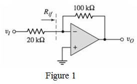
Figure P14.10
Want to see the full answer?
Check out a sample textbook solution
Chapter 14 Solutions
Microelectronics: Circuit Analysis and Design


- For the 4th order converter below, the switch stays at position "1" for a time equal to DT and at position "2" for a time equal to (T-DT), where D is the duty-cycle and T is the cycle-time. Assuming C₁ and C₂ very large, derive an expression for each of the following: 4₁ lin Vin C₁ HH + Vel 1) The voltage gain (V/Vin). 2) The input current (in) for 0 ≤ts T. 12 C₂ = HH 2 R + №º 1arrow_forwardThe arrow on the schematic symbol for a MOSFET indicates the channel material type. Select one: O True O False son The output of an op-amp comparator will be zero when both inputs are equal. Select one: of O True O False cion Which of the following current equations is true? Windos su of h lo le = 16 = Is ING D 40) ^ f4 f6 GD 19 O f2 f3 15 f7 18 (2) %23 & 3 E for GY K B Y N T of alt 61arrow_forward- V2 15Vdo 3 U1A R1 2 1k V- LM324 1k V3 15Vde | VOFF = 0 VAMPL = 1 FREQ = 2k AC = 0 0. R2 Figure 4. Operational amplifier circuit. What frequency does the output voltage (across R3) have? What is the amplitude of the output voltage? From the output waveform and the input waveform, determine the gain of the op-amp circuit. Does this match with what you predicted? How could you change this circuit so that the output voltage would be nearly the same as the input voltage? What purpose would that serve? Can you modify the existing circuit and verify this experimentally? What is the phase difference between the output and input voltage? Derive the transfer function for the output-input relationship for the operational amplifier. How would the gain and the output change if a capacitor were in the feedback path instead of a resistor? (Examine the circuit using phasors and impedance and circuit analysis techniques). -w-arrow_forward
- We examined the common source amplifier shown in the figure in the 5th experiment. The selection criterion of the input capacitance is Xcin = 0.1Rin: Calculate the required input capacitance value, Cin , if an input signal with a frequency of 2 kHz is applied. Şekitde gösterilen ortak source yükseltecini 5. deneyde incelemiştik Giriş kapasitesinin seçim kriteri Xcin - 0.1Rin dir. 2 kHzlik giriç sinyali için gerektt tapasite, Cm değerini hesaplayınız. Circuit parameters / Devre Parametreleri R1 = 53 k2, R, = 17 k2 R1 RD Cout Vout D VDD M2 Cin G Vin R2 RS cs O a. 74.19 nF O b. 86.55 nF O c. 49.46 nF O d. 61.82 nF O e. 43.28 nFarrow_forwardQ4 (a) The circuit shown in Figure Q4(a) is an oscillator. For this circuit: RF RA R VF R Figure Q4(a) Derive the expression for the feedback network, ß =E Vo (i) (ii) Determine the frequency of oscillation, and (iii) Find the ratio of Rf/RA to ensure the condition for oscillation is fulfilled. Design an astable multivibrator using 555 IC with a frequency of 50 kHz and 75% duty cycle. Label the circuit properly. (b)arrow_forwardFigure 1 shows the equivalent circuit of a voltage amplifier with a source and aload connected to its input and output, respectively. Suppose that the sourceinternal resistance is Rs = 5 kΩ, the amplifier input resistance is RIN = 95 kΩ, theamplifier gain is A = 100, the amplifier output resistance is ROUT = 150 Ω and theload resistance is RL = 5 kΩ. For a sinusoidal input with amplitude VS = 5 mV, whatis the amplitude of the voltage VL across the load resistor RL? What would thevoltage across the load be without the amplifier?arrow_forward
- Q19. For the circuit diagram shown in FigureB19. Vin and Vout corresponds to input and output voltage, V3 corresponds to output voltage from second stage of the circuit and A1, A2, A3 corresponds to Gain of each block. V3 =? Vin=3.5V Vout = 11.5dB Al- 6 A2-? A3-0.88 Figure B19 i) Compute the output voltage V3 and A2. ii) Whether the circuit in figure B19 will provide amplification or attenuation? Justify your answer.arrow_forwardQuestion 4. Design a C converter by drawing according to the values given below.The C ´uk converter has 24 V input and 36 V output providing 80 W load. In this case, choose Duty ratio, switching frequency, inductor dimensions so that the variation in inductor currents is not more than 5 percent of the average inductor current, output voltage fluctuation is less than 1 percent and voltage fluctuation at C1 is less than 5 percent.arrow_forwardA 3-bit binary weighted resistor DAC and a 3-bit R-2R ladder DAC have common values of Vref = 5V, R = 1kN, R = 2kN. Compare their output voltages for each of the following binary inputs. What do you observed? Binary Weighted Resistor DAC Resolution Binary input R-2R Ladder DAC Output voltage Resolution Output voltage 000 001 010 011 100 101 110 111arrow_forward
- Consider a Voltage-Voltage amplifier, input resistance (Rin) and output resistance (Rout) should be Microphone Amplifier Speaker Select one: Oa. none of these O b. Rin ∞ and Rout-00 O C. Rin and Rout-0 O d. Rin 0 and Rout→ ∞arrow_forwardQ/ Use The following circuit to design an oscillator of 5KHZ out The amplifier used in this oscillators is multistage C.S with Source resistance amplifier. The design must be with minimum No. of stages. use The following FET Parameter Id=2MA, gm= 2.5ms and rds= 40K ohm use VDD=24volt. Rarrow_forward(79) The Peak-to-Peak Output Voitage of a transistor-based is not limited by the Circuit used to amplify it. amplifier swort TRUE OR FALSE? b (1) A full-wave rectifier with a capacitor Filter will produce Perfect Dc voitage out Put TRUE OR FALSE?" Q ad Vac Ⓒ The Purpose of the Feedback resistor in a practical Integrator is to allow the low-freq gaim to become as Lage Possible AMOA al love as TRUE OR FALSEramato (®) et (@ Varrow_forward
 Introductory Circuit Analysis (13th Edition)Electrical EngineeringISBN:9780133923605Author:Robert L. BoylestadPublisher:PEARSON
 Delmar's Standard Textbook Of ElectricityElectrical EngineeringISBN:9781337900348Author:Stephen L. HermanPublisher:Cengage Learning
 Programmable Logic ControllersElectrical EngineeringISBN:9780073373843Author:Frank D. PetruzellaPublisher:McGraw-Hill Education
 Fundamentals of Electric CircuitsElectrical EngineeringISBN:9780078028229Author:Charles K Alexander, Matthew SadikuPublisher:McGraw-Hill Education
 Electric Circuits. (11th Edition)Electrical EngineeringISBN:9780134746968Author:James W. Nilsson, Susan RiedelPublisher:PEARSON
 Engineering ElectromagneticsElectrical EngineeringISBN:9780078028151Author:Hayt, William H. (william Hart), Jr, BUCK, John A.Publisher:Mcgraw-hill Education,