
Concept explainers
Videos
(a) Using the small-signal equivalent circuit in Figure 12.25 for the circuit in Figure
(a)
To derive: The expression for the small signal current gain of the circuit.
Answer to Problem 12.50P
The value of the small signal current gain is
Explanation of Solution
Given:
The given circuit is shown in Figure 1.
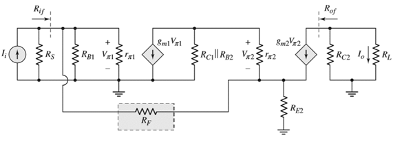
Figure 1
Calculation:
Mark the nodes and redraw the circuit.
The given diagram is shown in Figure 2
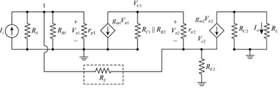
Figure 2
By KCL the expression for the current
The expression for the node voltage is given by,
Apply KCL at node
Substitute
The expression for the output current is given by,
Apply KCL at node
Substitute
Substitute
Consider
Thus, the expression for the small signal current gain is,
Conclusion:
Therefore, the value of the small signal current gain is
(b)
The value of the gain
To compare: The obtained value with the given value of gain. and compare it to the value of 9.58.
Answer to Problem 12.50P
The value of the current gain is
Explanation of Solution
Given:
The given circuit is shown below.

The given value of gain is 9.58.
Also, the values are:
Calculation:
The expression to determine the value of the resistance
The expression for the value of the voltage
The expression to determine the value of the current
Substitute
The value of the current
Substitute
The expression to determine the value of the resistance
The value of the Thevenin voltage is given by,
The expression to determine the value of the current
Substitute
The value of the current
Substitute
The expression to determine the transconductance of first transistor is calculated as,
The expression to determine the transconductance of second transistor is calculated as,
The value of the small signal input resistance is calculated as,
The value of the small signal input resistance is calculated as,
The value of A is calculated as,
The value of B is calculated as,
The value of C is calculated as,
The value of D is calculated as,
Substitute
Substitute
The value of the current gain is
Want to see more full solutions like this?
Chapter 12 Solutions
Microelectronics: Circuit Analysis and Design


- Not use ai pleasearrow_forward49. For the circuit below, what is the best connection of the capacitor to filte voltage? ბი DO A O BO wwwww wwwww M m H E LOADarrow_forward5.25. Determine the corner frequency resulting from Cin in Fig. 5.47(d). For simplicity, assume C₁ is a short circuit. TVDD C₁ M2 RF Vin H w - Vout Cin M₁arrow_forward
- In the below circuit, find out the value of equivalent Thevenin's voltage and Thevenin's resistance at the terminal. 2000 0.25 A 400 2 800 2 0.1 Aarrow_forwardQ1: For the circuit shown in Figure-1, (a) Calculate the equivalent resistance of the circuit, RAB at the terminals A and B. [10] (b) When 50V dc source is switched at terminals A-B, solve for the voltage V₁ at the location shown. [10] 50V www 12Ω 10Ω 5Ω www www A + B 200 Figure-1 www 10Ω ww 25Ω 100arrow_forwarda. Write a PLC ladder diagram that allows the teacher to teach AND, OR, and XOR logic gates through using three PLC's digital input points and only one digital output point.arrow_forward
- rately by PRACTICE 4.2 For the circuit of Fig. 4.5, compute the voltage across each curren source. 202 ww 3A 30 ww 4Ω S 50 www Reference node FIGURE 4.5 Ans: V3A =5.235 V; 7A = 11.47 V. 7 Aarrow_forwardQ2) a) design and show me your steps to convert the following signal from continuous form to digital form: s(t)=3sin(3πt) -1 373 Colesarrow_forwardA sequence is defined by the relationship r[n] = [h[m]h[n+m]=hn*h-n where h[n] is a minimum-phase sequence and r[n]= 4 4 (u[n]+ 12" [n-1] 3 (a) Find R(z) and sketch the pole-zero diagram. (b) Determine the minimum-phase sequence h[n] to within a scale factor of ±1. Also, determine the z-transform H(z) of h[n].arrow_forward
- usıng j-k and D flipflop design a counter that counts 0,2,1 again as shown below ın the tablearrow_forwardfind the minterms of the followıng boolean expressıon desıgn F's cırcuit using one of the approciate decoders given below and a NOR gateF(A,B,C,D)=(A+'BC)(B 'C+'A 'D + CD)arrow_forward64) answer just two from three the following terms: A) Design ADC using the successive method if the Vmax=(3) volt, Vmin=(-2) volt, demonstrate the designing system for vin-1.2 volt. Successive Approximation ADC Input Voltage-1.1 V -4-3.5-3 -2.5 -2 -1.5 +1 -0.5 0 0.5 1 1.5 2 2.5 3 3.5 1 T -8 -7 -6 -5 -3 +2 -1 0 1 2 3 4 5 6 7 X=1??? 1st guess: -0.25 V (too high) X=11?? 2nd guess: -2.25 V (too low) 3rd guess: -1.25 V (too low) X=1110 X=111? 4th guess: -0.75 V (too high) Make successive guesses and use a comparator to tell whether your guess is too high or too low. Each guess determines one bit of the answer and cuts the number of remaining possibilities in half.arrow_forward
 Introductory Circuit Analysis (13th Edition)Electrical EngineeringISBN:9780133923605Author:Robert L. BoylestadPublisher:PEARSON
 Delmar's Standard Textbook Of ElectricityElectrical EngineeringISBN:9781337900348Author:Stephen L. HermanPublisher:Cengage Learning
 Programmable Logic ControllersElectrical EngineeringISBN:9780073373843Author:Frank D. PetruzellaPublisher:McGraw-Hill Education
 Fundamentals of Electric CircuitsElectrical EngineeringISBN:9780078028229Author:Charles K Alexander, Matthew SadikuPublisher:McGraw-Hill Education
 Electric Circuits. (11th Edition)Electrical EngineeringISBN:9780134746968Author:James W. Nilsson, Susan RiedelPublisher:PEARSON
 Engineering ElectromagneticsElectrical EngineeringISBN:9780078028151Author:Hayt, William H. (william Hart), Jr, BUCK, John A.Publisher:Mcgraw-hill Education,