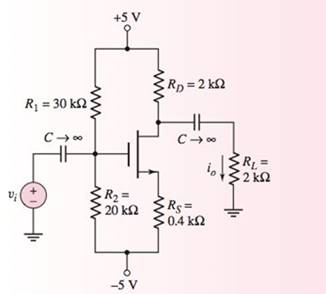
For the circuit in Figure 12.31, the transistor parameters are K n = 2 mA / V 2 , V T N = 2 V , and λ = 0. (a) Determine (i) I D Q and (ii) the transconductance transfer function A g f = i o / v i . (b) If the conductance parameter decreases by 10 percent to K n = 1.8 mA / V 2 , determine (i) the new value of I D Q and (ii) the percent change in A g f . (Ans. (a) (i) I D Q = 2.31 mA , (ii) A g f = − 0.7904 mA / V ; (b) (i) I D Q = 2.22 mA , (ii) − 2.68 % ) Figure 12.13 Figure for Exercise Ex 12.11
For the circuit in Figure 12.31, the transistor parameters are K n = 2 mA / V 2 , V T N = 2 V , and λ = 0. (a) Determine (i) I D Q and (ii) the transconductance transfer function A g f = i o / v i . (b) If the conductance parameter decreases by 10 percent to K n = 1.8 mA / V 2 , determine (i) the new value of I D Q and (ii) the percent change in A g f . (Ans. (a) (i) I D Q = 2.31 mA , (ii) A g f = − 0.7904 mA / V ; (b) (i) I D Q = 2.22 mA , (ii) − 2.68 % ) Figure 12.13 Figure for Exercise Ex 12.11
Solution Summary: The author calculates the value of the drain current I_DQ and the trans-conductance transfer function.
For the circuit in Figure 12.31, the transistor parameters are
K
n
=
2
mA
/
V
2
,
V
T
N
=
2
V
,
and
λ
=
0.
(a) Determine (i)
I
D
Q
and (ii) the transconductance transfer function
A
g
f
=
i
o
/
v
i
.
(b) If the conductance parameter decreases by 10 percent to
K
n
=
1.8
mA
/
V
2
,
determine (i) the new value of
I
D
Q
and (ii) the percent change in
A
g
f
. (Ans. (a) (i)
I
D
Q
=
2.31
mA
, (ii)
A
g
f
=
−
0.7904
mA
/
V
;
(b) (i)
I
D
Q
=
2.22
mA
,
(ii)
−
2.68
%
)
Consider the circuit of Figure 12.7 on page 605. Assume that VCC=20 V, VBB=0.3 V, RB=40 kΩ, and RC=2 kΩ. The input signal is a 0.2-V-peak 1-kHz sinusoid given by vin(t)=0.2 sin(2000πt). The common-emitter characteristics for the transistor are shown in Figure P12.18. Determine the maximum, minimum, and Q-point values for vCE. What is the approximate voltage gain for this circuit? Why is the gain so small in magnitude?
........
(Figure-1)
R.
RB= 380kN,Rc= 1kN
B = 100, VBB = Vcc=12V
RB
ww
Vec
CC
.........
I,
V CE
СЕ
V
ВЕ
BB
Q-1-b) Describe briefly the input / output characteristics and application of Common
Emitter BJT Configuration
4. The transistor is a three-layer semiconductor device consisting of either - of material or
5. The input set for the common-base amplifier relates an input current
various levels of output voltage
6. For BJT transistor ICBO =0.02 mA and ICEO= 4---- if B =60
to an input voltage
for
-----
----
Need a deep-dive on the concept behind this application? Look no further. Learn more about this topic, electrical-engineering and related others by exploring similar questions and additional content below.


 Introductory Circuit Analysis (13th Edition)Electrical EngineeringISBN:9780133923605Author:Robert L. BoylestadPublisher:PEARSON
 Delmar's Standard Textbook Of ElectricityElectrical EngineeringISBN:9781337900348Author:Stephen L. HermanPublisher:Cengage Learning
 Programmable Logic ControllersElectrical EngineeringISBN:9780073373843Author:Frank D. PetruzellaPublisher:McGraw-Hill Education
 Fundamentals of Electric CircuitsElectrical EngineeringISBN:9780078028229Author:Charles K Alexander, Matthew SadikuPublisher:McGraw-Hill Education
 Electric Circuits. (11th Edition)Electrical EngineeringISBN:9780134746968Author:James W. Nilsson, Susan RiedelPublisher:PEARSON
 Engineering ElectromagneticsElectrical EngineeringISBN:9780078028151Author:Hayt, William H. (william Hart), Jr, BUCK, John A.Publisher:Mcgraw-hill Education,