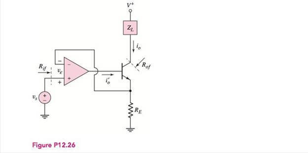
Consider the circuit in Figure P12.26. The input resistance of the op-amp is R i = ∞ and the output resistance is R o = 0. The op-amp has a finite gain, so that i o ′ = A g v ε . The current gain of the transistor is h F E . (a) Write the closed-loop transfer function in the form A g f = i o v s = A g ( 1 + β z A g ) where A g is the open-loop gain of the system. (b) What is the expression for β z ? ( c ) If A g = 5 × 10 5 mS and A g f = 10 mS , what is the required β z and R E ? ( d ) If A g increases by 10 percent, what is the corresponding percent change in A g f Figure P12.26
Consider the circuit in Figure P12.26. The input resistance of the op-amp is R i = ∞ and the output resistance is R o = 0. The op-amp has a finite gain, so that i o ′ = A g v ε . The current gain of the transistor is h F E . (a) Write the closed-loop transfer function in the form A g f = i o v s = A g ( 1 + β z A g ) where A g is the open-loop gain of the system. (b) What is the expression for β z ? ( c ) If A g = 5 × 10 5 mS and A g f = 10 mS , what is the required β z and R E ? ( d ) If A g increases by 10 percent, what is the corresponding percent change in A g f Figure P12.26
Solution Summary: The author describes an inverting operational amplifier circuit with finite gain and infinite input and output impedances. The closed loop transconductance gain is represented as A_gf and it is calculated
Consider the circuit in Figure P12.26. The input resistance of the op-amp is
R
i
=
∞
and the output resistance is
R
o
=
0.
The op-amp has a finite gain, so that
i
o
′
=
A
g
v
ε
.
The current gain of the transistor is
h
F
E
.
(a) Write the closed-loop transfer function in the form
A
g
f
=
i
o
v
s
=
A
g
(
1
+
β
z
A
g
)
where
A
g
is the open-loop gain of the system. (b) What is the expression for
β
z
?
(
c
)
If
A
g
=
5
×
10
5
mS
and
A
g
f
=
10
mS
,
what is the required
β
z
and
R
E
?
(
d
)
If
A
g
increases by 10 percent, what is the corresponding percent change in
A
g
f
Q. One advantage of having feedback in op amp circuit is
A. low gain
B. low bandwidth
C. can control gain
D. high output voltage
E. less input signal
F. less complicated
Construct the signal flow graph for the following set of simultaneous equations: X₂ = A21 X₁ + A23
X3, X3 = A31 X1 + A32 X2 + A33 X3, X4 = A42X2 + A43X3. Identify the (a) input node, (b) output node, (c)
forward paths, (d) feedback paths, and (e) self-loop.
Project # 3 (Use a FET op-amp) You’ve been working with an implementation team to build the following components of a system: The system consists of a DC power supply, filters, instrumentation amplifier, one-state system and A/D converter. Build an AC/DC dual power supply circuit that draws a 55Vp-p sinusoidal voltage, to provide a dc output voltage of +10 V. Find the proper data sheet of the IC regulator and specify ranges of output current and voltage. Full analysis of voltages and currents should be included. What modifications would you recommend to draw more current while maintaining same output voltage? Build a 4th order Butterworth LP filters that cover a signal range 10kHz and a gain of 100V/V each. Use C = 0.01µF with proper values of R’s. Record your findings and include plots (magnitude and phase. Calculate the roll-off of the filter. Build an instrumentation amplifier having a differential gain of 50V/V. Choose the right differential input and common input signals to…
Need a deep-dive on the concept behind this application? Look no further. Learn more about this topic, electrical-engineering and related others by exploring similar questions and additional content below.


 Introductory Circuit Analysis (13th Edition)Electrical EngineeringISBN:9780133923605Author:Robert L. BoylestadPublisher:PEARSON
 Delmar's Standard Textbook Of ElectricityElectrical EngineeringISBN:9781337900348Author:Stephen L. HermanPublisher:Cengage Learning
 Programmable Logic ControllersElectrical EngineeringISBN:9780073373843Author:Frank D. PetruzellaPublisher:McGraw-Hill Education
 Fundamentals of Electric CircuitsElectrical EngineeringISBN:9780078028229Author:Charles K Alexander, Matthew SadikuPublisher:McGraw-Hill Education
 Electric Circuits. (11th Edition)Electrical EngineeringISBN:9780134746968Author:James W. Nilsson, Susan RiedelPublisher:PEARSON
 Engineering ElectromagneticsElectrical EngineeringISBN:9780078028151Author:Hayt, William H. (william Hart), Jr, BUCK, John A.Publisher:Mcgraw-hill Education,