Digital Fundamentals (11th Edition)
11th Edition
ISBN: 9780132737968
Author: Thomas L. Floyd
Publisher: PEARSON
expand_more
expand_more
format_list_bulleted
Videos
Textbook Question
Chapter 3, Problem 20P
As you have learned, the two logic symbols shown in Figure 3-86 represent equivalent operations. The difference between the two is strictly from a functional viewpoint. For the NAND symbol, look for two HIGHs on the inputs to give a LOW output. For the negative-OR, look for at least one LOW on the inputs to give a HIGH on the output. Using these two functional viewpoints, show that each gate will produce the same output for the given inputs
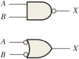
Figure 3-86
Expert Solution & Answer
Want to see the full answer?
Check out a sample textbook solution
Students have asked these similar questions
One logic function that is used for a variety of purposes (including within adders and to compute parity) is exclusive OR. The output of a two-input exclusive OR function is true only if exactly one of the inputs is true. Show the truth table for a two-input exclusive OR function and implement this function using AND gates, OR gates, and inverters.
draw the logic diagrams (using gates) of the positive-edge triggered T and JK flip-flops
understand how flip flops are working by poking the inputs and then practically obtain the function tables of the T and JK flip-flops;
Given the Boolean function F (X, Y, Z) = ABC + AB’ + A’ C’
derive the logic circuit that is used to implement the above Boolean function using the multiplixer (use the logic symbol of the MUX)
Using the EWB software, implement the circuit that you obtained in step 1. Verify your answer.
Chapter 3 Solutions
Digital Fundamentals (11th Edition)
Ch. 3.1 - When a 1 is on the input of an inverter, what is...Ch. 3.1 - An active-HIGH pulse (HIGH level when asserted,...Ch. 3.2 - When is the output of an AND gate HIGH?Ch. 3.2 - When is the output of an AND gate LOW?Ch. 3.2 - Describe the truth table for a 5-input AND gate.Ch. 3.3 - When is the output of an OR gate HIGH?Ch. 3.3 - When is the output of an OR gate LOW?Ch. 3.3 - Describe the truth table for a 3-input OR gate.Ch. 3.4 - When is the output of a NAND gate LOW?Ch. 3.4 - When is the output of a NAND gate HIGH?
Ch. 3.4 - Describe the functional differences between a NAND...Ch. 3.4 - Write the output expression for a NAND gate with...Ch. 3.5 - When is the output of a NOR gate HIGH?Ch. 3.5 - When is the output of a NOR gate LOW?Ch. 3.5 - Describe the functional difference between a NOR...Ch. 3.5 - Write the output expression for a 3-input NOR with...Ch. 3.6 - When is the output of an XOR gate HIGH?Ch. 3.6 - When is the output of an XNOR gate HIGH?Ch. 3.6 - How can you use an XOR gate to detect when two...Ch. 3.7 - List six process technologies used for...Ch. 3.7 - What does the term volatile mean in relation to...Ch. 3.7 - What are two design entry methods for programming...Ch. 3.7 - Prob. 4CUCh. 3.7 - Write a VHDL description of a 3-input NOR gate,Ch. 3.7 - Write a VHDL description of an XOR gate.Ch. 3.8 - How is fixed-function logic different than PLD...Ch. 3.8 - Prob. 2CUCh. 3.8 - Identify the following IC logic designators: LS HC...Ch. 3.8 - Prob. 4CUCh. 3.8 - What does the term hex inverter mean? What does...Ch. 3.8 - A positive pulse is applied to an inverter input....Ch. 3.8 - A certain gate has a propagation delay time of 6...Ch. 3.8 - Prob. 8CUCh. 3.8 - Prob. 9CUCh. 3.8 - Prob. 10CUCh. 3.9 - Prob. 1CUCh. 3.9 - If two different input waveforms are applied to a...Ch. 3.9 - Prob. 3CUCh. 3 - An inverter performs the NOR operation.Ch. 3 - An AND gate can have only two inputsCh. 3 - If any input to an OR is 1, the output is 1.Ch. 3 - If all inputs to an AND gate are 1, the output is...Ch. 3 - A NAND gate has an output that is opposite the...Ch. 3 - A NOR gate can be considered as an OR gate...Ch. 3 - The output of an exclusive-OR is 0 if the inputs...Ch. 3 - Prob. 8TFQCh. 3 - Once programmed, PLD logic can be changed.Ch. 3 - Fan-out is the number of similar gates that a...Ch. 3 - When the input to an inverter is HIGH (1), the...Ch. 3 - An inverter performs an operation known as...Ch. 3 - The output of an AND gate with inputs A, B, and C...Ch. 3 - The output of an OR gate with inputs A, B, and C...Ch. 3 - A pulse is applied to each input of a 2-input NAND...Ch. 3 - A pulse is applied to each input of a 2-input NOR...Ch. 3 - A pulse is applied to each input of an...Ch. 3 - Prob. 8STCh. 3 - The purpose of a programmable link in an AND array...Ch. 3 - The term OTP means open test point one-time...Ch. 3 - Prob. 11STCh. 3 - Prob. 12STCh. 3 - Two ways to enter a logic design using PLD...Ch. 3 - Prob. 14STCh. 3 - In-system programming of a PLD typically utilizes...Ch. 3 - To measure the period of a pulse waveform, you...Ch. 3 - Prob. 17STCh. 3 - The input waveform shown in Figure 3-76 is applied...Ch. 3 - A combination of inverters is shown in Figure...Ch. 3 - If the waveform in Figure 3-76 is applied to point...Ch. 3 - Draw the rectangular outline symbol for a 4-input...Ch. 3 - Determine the output, X, for a 2-input AND gate...Ch. 3 - Repeat problem 5 for the waveforms in Figure 3-79Ch. 3 - The input wave forms applied to a 3-input AND gate...Ch. 3 - The input waveforms applied to a 4-input AND gate...Ch. 3 - Draw the rectangular outline symbol for a 3-input...Ch. 3 - Write the expression for a 5-input OR gate with...Ch. 3 - Determine the output for a 2-input OR gate when...Ch. 3 - Repeat Problem 7 for a 3-input OR gate.Ch. 3 - Repeat Problem 8 for a 4-input OR gate.Ch. 3 - For the five input waveforms in Figure 3-8219,...Ch. 3 - Draw the rectangular outline symbol for a 4-input...Ch. 3 - Show the truth table for a 3-input OR gate.Ch. 3 - For the set of input waveforms in Figure 3-83,...Ch. 3 - Determine the gate output for the input waveforms...Ch. 3 - Determine the output waveform in Figure 3-8513Ch. 3 - As you have learned, the two logic symbols shown...Ch. 3 - Repeat Problem 17 for a 2-input NOR gate.Ch. 3 - Determine the output waveform in Figure 3-87 and...Ch. 3 - Repeat Problem 19 for a 4-input NOR gate.Ch. 3 - The NAND and the negative-OR symbols represent...Ch. 3 - How does an exclusive-OR gate differ from an OR...Ch. 3 - Repeat Problem 17 for an exclusive-OR gate.Ch. 3 - Repeat Problem 17 for an exclusive-NOR gateCh. 3 - Determine the output of an exclusive-OR gate for...Ch. 3 - In the simple programmed AND array with...Ch. 3 - Determine by row and column number which fusible...Ch. 3 - Describe a 4-input AND gate using VHDL.Ch. 3 - Describe a 5-input NOR gate using VHDLCh. 3 - In the comparison of certain logic devices, it is...Ch. 3 - Prob. 34PCh. 3 - Determine tPLHandtPHL from the oscilloscope...Ch. 3 - Prob. 36PCh. 3 - If a logic gate operates on a dc supply voltage of...Ch. 3 - The variable ICCH represents the dc supply current...Ch. 3 - Examine the conditions indicated in Figure 3-92,...Ch. 3 - Determine the faulty gates in Figure 3-93 by...Ch. 3 - Using an oscilloscope, you make the observations...Ch. 3 - Prob. 42PCh. 3 - Every time the ignition switch is turned on in the...Ch. 3 - What failure(s) would you suspect if the output of...Ch. 3 - Modify the frequency counter in Figure 3-16 to...Ch. 3 - Prob. 46PCh. 3 - Design a circuit to fit in the beige block of...Ch. 3 - Modify the logic circuit for the intrusion alarm...Ch. 3 - Further modify the logic circuit from Problem 48...Ch. 3 - Sensors are used to monitor the pressure and the...Ch. 3 - In a certain automated manufacturing process,...Ch. 3 - Open file P03-52. For the specified fault, predict...Ch. 3 - Open file P03-53. For the specified fault, predict...Ch. 3 - Open file P03-54. For the observed behavior...Ch. 3 - Open file P03-55. For the observed behavior...
Additional Engineering Textbook Solutions
Find more solutions based on key concepts
What is the output of the following code? double a [3] = {1.1, 2.2, 3.3}; cout a [0] a [1] a[2] endl;...
Problem Solving with C++ (9th Edition)
What is the difference between a class and an object?
Computer Science: An Overview (12th Edition)
Write a program that calculates the sum of the digits of an integer. For example, the sum of the digits of the ...
Programming in C
For each of the following activities, give a PEAS description of the task environment and characterize it in te...
Artificial Intelligence: A Modern Approach
Write a program to read a list of nonnegative integers and to display the largest integer, the smallest integer...
Java: An Introduction to Problem Solving and Programming (8th Edition)
Describe the common components needed to create a Web-based application.
Modern Database Management (12th Edition)
Knowledge Booster


Learn more about
Need a deep-dive on the concept behind this application? Look no further. Learn more about this topic, computer-science and related others by exploring similar questions and additional content below.Similar questions
- Consider the following operation: Z = AB · BC a. Write out the truth table for the given expression. b. Draw and design a logic circuit that implements the given expression using 6 NMOS devices only. Draw the logic gates diagram first. Use 2-input logic gates only. No need to indicate values for the supply voltage and pull-up resistors. (Hint: You need to manipulate and rewrite expression Z using De Morgan's theorem). c. Given a supply voltage of 5V and assuming low states to be OV, redraw the equivalent circuit and label all important voltages when A=5V, B=5V, and C=5V.arrow_forwardFirst, you must create a logic circuit using only basic gates such as AND, OR, NOR, NAND, NOT, etc. to implement an ADDER capable of adding two 4 bit binary numbers. Second, you must create a logic circuit using only basic gates such as AND, OR, NOR, NAND, NOT, etc. to implement a Subtractor that is capable of subtracting the second number from the first, by converting the second number into its 2's complement form and then adding the resulting number to the first number. You do not need to worry about accomodating the addition or subtraction of negative numbers. Finally, create a limited ALU (Arithmetic logic unit) circuit using Logism that implements a Full Adder circuit capable of adding 2 – 4 bit binary numbers and subtracting 2- 4 bit binary numbers. Also, implement the ability to select a bitwise AND operation and a bitwise OR operation. For the ALU it is acceptable to use the Adder and Subtractor circuits that are listed under the "Arithmetic" folder in Logism. (Logism tips and…arrow_forward2. Consider the circuit below. a. Write the Boolean expression for output F in terms of A, B and C. b. Construct a truth table for the circuit with A as MSB and C as LSB. c. Write the Canonical SOP and POS forms for output F. A B C 3. Draw the logic circuit represented by the expression F(A, B) = AB using no more than 5 units of 2-input NAND gate and write the corresponding Boolean expression.arrow_forward
- Question 1 ( Given the logic expressions for a set of digital circuits with four inputs (a, b, c, and d) and three outputs (F, G and H): a) Use K-map to simplify the expression for output F only and write down the logic expression in SOP. Implement the circuit using on NAND gates. b) Use VEM (variable entered mapping) to simplify the expressions for output G only. Draw the VEM K-map and write down the reduced logic expression. You are to use the least significant bit (d) as your variable. Implement the circuit using any gates of your choice. c) Use the Quine-McCluskey method to simplify the expression for output H only, and write down the logic expression. Implement the circult using only 2:1 mux devices. d) Implement the circuits for all three outputs (F, G and H) using three 8-1 mux devices (in one diagram). Hints: please show all your working and justify how you get your results No. 0 1 2 3 4 5 6 7 8 9 10 11 12 13 14 15 Input abed 0000 0 0 0001 1 0 0 1 0010 0011 0 0100 0101 0110…arrow_forwardThe gates in the exclusive-OR circuit below have delays of 2 ns for the inverter, 5 ns for the AND gate, and 7 ns for the OR gate. The circuit's input goes from xy = 10 to xy = 11. Determine the signals at the output of each gate from t = 0 to t = 60 ns.arrow_forwardQuestion 1 Implement the following logic functions using BJTs. Use the S-Model. Both input and output should be voltage signals OUT= A.B + C OUT = A.B + A.Barrow_forward
- You have to design a logic diagram which can implement the complement of following by using NAND gates ONLY. F (A, B, C, D) = Σ (0, 1, 2, 3, 6, 10, 11, 14)arrow_forwardDesign a logic circuit whose output is HIGH only when a majority of inputs A, B, and C are LOW. Draw the circuit using all NAND gates.arrow_forwardQuestion 2: A combinational circuit has 4 inputs (A, B, C, D) and 1 output (F). ABCD represent a majority function. The output of the majority function is equal to 1 if the input variables have more 1's than O's, otherwise the output is 0. a. Construct the truth table of the required circuit. b. Implement the minimized expression of F using 3-level all NAND gate circuit. Implement a 2-1Multiplexer using three-state buffers.arrow_forward
- Write the Boolean expression for a four-input NAND gate and apply DeMorgan theorem. Draw the circuit diagram of four-input NAND gate using two input NAND gates. You may need additional logic gates to complete the diagram.arrow_forwardAnswer the following questions: If a 3-input XOR gate has eight input possibilities, how many of those possibilities will result in a HIGH output? What type of logic circuit is represented by the figure 4 shown below? Name the gate whose output is HIGH if and only if all the inputs are LOW If a JK latch has J=1, K=0 initially. When the K input goes high, what will be the output?arrow_forwardGiven a 4-bit signed integer, design a circuit that outputs its absolute value. You can assume that the input will always have a valid output. (a) Draw a logic diagram of this circuit. You may use 4-bit half adder(s), 2x1 4-bit multiplexer(s), and any logic gate(s) in your design. (b) With the following Verilog code, implement your design above in Verilog. module half_adder (input [3:0] a, input [3:0] b, output [3:0] s); assign s = a + b; endmodule module mux(input [3:0] D0, input [3:0] D1, input S, output reg [3:0] O); always @(*) begin if (S == 0) O = D0; else if (S == 1) O = D1; else O = 4’bx; end endmodulearrow_forward
arrow_back_ios
SEE MORE QUESTIONS
arrow_forward_ios
Recommended textbooks for you
 Database System ConceptsComputer ScienceISBN:9780078022159Author:Abraham Silberschatz Professor, Henry F. Korth, S. SudarshanPublisher:McGraw-Hill Education
 Starting Out with Python (4th Edition)Computer ScienceISBN:9780134444321Author:Tony GaddisPublisher:PEARSON
 Digital Fundamentals (11th Edition)Computer ScienceISBN:9780132737968Author:Thomas L. FloydPublisher:PEARSON
 C How to Program (8th Edition)Computer ScienceISBN:9780133976892Author:Paul J. Deitel, Harvey DeitelPublisher:PEARSON
 Database Systems: Design, Implementation, & Manag...Computer ScienceISBN:9781337627900Author:Carlos Coronel, Steven MorrisPublisher:Cengage Learning
 Programmable Logic ControllersComputer ScienceISBN:9780073373843Author:Frank D. PetruzellaPublisher:McGraw-Hill Education
Database System Concepts
Computer Science
ISBN:9780078022159
Author:Abraham Silberschatz Professor, Henry F. Korth, S. Sudarshan
Publisher:McGraw-Hill Education
Starting Out with Python (4th Edition)
Computer Science
ISBN:9780134444321
Author:Tony Gaddis
Publisher:PEARSON
Digital Fundamentals (11th Edition)
Computer Science
ISBN:9780132737968
Author:Thomas L. Floyd
Publisher:PEARSON
C How to Program (8th Edition)
Computer Science
ISBN:9780133976892
Author:Paul J. Deitel, Harvey Deitel
Publisher:PEARSON
Database Systems: Design, Implementation, & Manag...
Computer Science
ISBN:9781337627900
Author:Carlos Coronel, Steven Morris
Publisher:Cengage Learning
Programmable Logic Controllers
Computer Science
ISBN:9780073373843
Author:Frank D. Petruzella
Publisher:McGraw-Hill Education
Boolean Algebra - Digital Logic and Logic Families - Industrial Electronics; Author: Ekeeda;https://www.youtube.com/watch?v=u7XnJos-_Hs;License: Standard YouTube License, CC-BY
Boolean Algebra 1 – The Laws of Boolean Algebra; Author: Computer Science;https://www.youtube.com/watch?v=EPJf4owqwdA;License: Standard Youtube License